Document Number: 002-14826 Rev. *G
Page 60 of 65
PRELIMINARY
CYW43903
18. Power-Up Sequence and Timing
18.1 Sequencing of Reset and Regulator Control Signals
The CYW43903 has two signals that allow the host to control power consumption by enabling or disabling the internal regulator blocks.
These signals are described below. Additionally, diagrams are provided to indicate proper sequencing of the signals for various
operational states (see
). The timing values indicated are minimum required values; longer delays are also
acceptable.
18.1.1 Description of Control Signals
■
REG_ON
: Used by the PMU to power-up the CYW43903. It controls the internal CYW43903 regulators. When this pin is high,
the regulators are enabled and the device is out of reset. When this pin is low the regulators are disabled.
■
HIB_REG_ON_IN
: Used by the Hibernation (HIB) block to power up the internal CYW43903 regulators. If the HIB_REG_ON_IN
pin is low, the regulators are disabled. For the HIB_REG_ON_IN pin to work as designed, HIB_REG_ON_OUT must be con-
nected to REG_ON.
Note:
The CYW43903 has an internal power-on reset (POR) circuit. The device will be held in reset for a maximum of 110 ms after
VDDC and VDDIO have both passed the POR threshold.
Note:
The 10%–90% VBAT rise time should not be faster than 40 microseconds. VBAT should be up before or at the same time as
VDDIO. VDDIO should not be present first or be held high before VBAT is high.
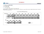
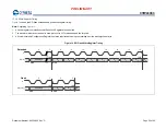
18.1.2 Control Signal Timing Diagrams
Figure 18. REG_ON = High, No HIB_REG_ON_OUT Connection to REG_ON
Figure 19. HIB_REG_ON_IN = High, HIB_REG_ON_OUT Connected to REG_ON
3 2 .6 7 8 k H z
S le e p C lo ck
V B A T
V D D IO
R E G _ O N
H IB _ R E G _ O N _ IN
~ 2 S le e p C y cle s
3 2 .6 7 8 k H z
S le e p C lo ck
V B A T
V D D IO
H IB _ R E G _ O N _ IN
~ 2 S le e p C y cle s


