


User Manual
15 of 29
Revision 1.0
2019-09-18
EVAL-M1-2ED2106S User Manual
2ED2106S06F drive board for BLDC motor
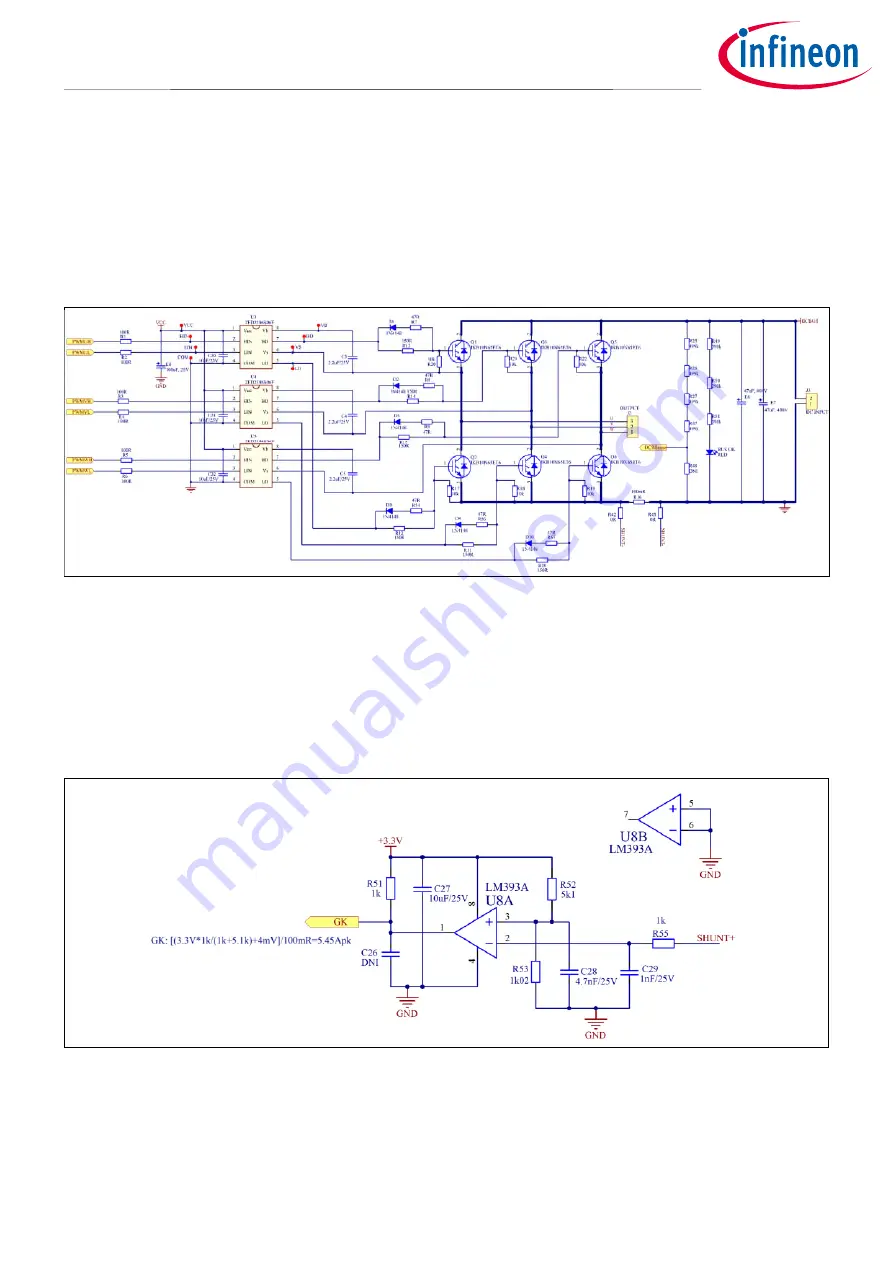
Circuit diagram of the EVAL-M1-2ED2106S
7.2
Main power circuit
The gate drivers and IGBTs is designed as Figure 9. Each PWM signal to the gate driver’s input involves a resistor
in series to suppress the noise induced from the ground bouncing while the IGBT switching. The ON and OFF
gate resistors are separated for an optimized tradeoff between the IGBT switching loss and system EMI
performance.
The DC bus status is sampled by a resistor divider.
Figure 9
Main power circuit
7.3
OCP circuit
The overcurrent protection (OCP) function is necessary for motor drive applications. As configured in Figure 10,
the output of the comparator LM393A shall flip-flop low when the single-shunt current is over 5.45 A. The
generated gate kill (GK) signal is sent to the controller IC disabling all the gate driver PWM inputs to turn off the
IGBTs.
Figure 10 OCP circuit