


QUICK START GUIDE
Evaluation Boards EPC9179/80/81
EPC – POWER CONVERSION TECHNOLOGY LEADER |
| ©2023 | For more information:
| 7
Potentiometer P1 is used to adjust this turn-off delay and the resulting
output pulse width, with clockwise rotation increasing the pulse width
applied to the gate of Q1. Note that the minimum delay setting causes
both turn-on and turn-off paths to have an approximately equal delay,
which would result in a zero-width pulse. Since the gate driver U3 has a
minimum pulse width specification of > 1 ns, it is U3 that determines the
minimum attainable output pulse width. Small errors in the delay path
do not significantly impact the output. The maximum pulse width that
can be obtained with the NPG is approximately 60 ns, so if longer pulses
are needed, the NPG should be disabled.
When using the NPG, it is recommended that the input pulse should be
at least 10 ns longer than the desired output pulse to guarantee reliable
operation under all ambient conditions.
ADVANCED FEATURES
The EPC9179/80/81 has the option to be controlled from a differential
input. As shipped, this input is configured for standard LVDS signals.
It input is available to the user through the 8-pin header J11. Table 4
shows the pinout for J11, which also provides alternate access to some
of the power supply voltages on the board. In order to enable the LVDS
or other differential input, move the jumper on J10 to the upper position
(Figure 6).
LVDS AND ALTERNATE INPUTS
The following features require modifications to the board.
Load Clamping diodes
Empty component footprints are present on the EPC9179/80/81 to allow
the user to mount up to 3 clamp diodes (D1, D2, D3). While such diodes
can provide some protection to FET Q1 and laser or load U1, they have
parasitic inductance and capacitance that can reduce performance.
In addition, they clamp the laser or load reverse voltage and this can
reduce turn-off speed. Hence, they are not populated, and it is left to the
user to determine whether they are useful for a particular application.
Eye safe operation
In some applications, it is required that the driver remain eye-safe in
the event of a failure causing Q1 to be on in an uncontrolled manner,
e.g. an erroneous gate drive signal or FET short. While the charging
resistance provides some current limiting, it may not be enough. In
such a case, R8 can be removed, and at least one of the clamp diodes
D1, D2, or D3 populated. Once this is done, the capacitor bank will
be charged through the charging resistance and the clamp diode(s).
However, if Q1 is on, the charging current will now flow through Q1
and not the laser diode, preventing any light output.
Fast Refresh
The value of the energy storage cap {C2, C3, C4, C5, C6} can be modified
as desired, as well as the recharge resistor {R4, R5, R6, R7}. In the extreme
case, the resistor may be reduced to 0 Ω for cases where a capacitive
discharge pulse is not desired. The latter can also be accomplished
by populating R1. If this approach is taken, it is recommended that R1
have some small value of resistance (5 Ω to 20 Ω) to damp possible
resonances in the power bus.
Logic input level and type
The input specification of the demo board may also be modified. For
single-ended inputs, the input logic level can be reduced from 3.3 V
logic to 2.5 V or 1.8 V by changing R37. Please see the U7 datasheet for
further details. If a differential input different than LVDS is desired, the
differential receiver U8 can accommodate sub-LVDS, CML or LVPECL
signals by changing the values of U8’s input termination network.
Please see the U8 datasheet for further details.
Improving laser cooling
Some pulse laser applications are thermally limited by laser power
dissipation. Usually, the laser die substrate forms the cathode, which is
attached to the drain of Q1. Since this terminal is the most electrically
active terminal in the whole circuit, it must be kept small and electrically
isolated from anything else in the circuit. This makes it difficult for heat
to flow out of the laser. This terminal is connected to a small copper
land on the bottom of the PCB with a thermally conductive via array.
Hence, the thermal resistance from the laser cathode to the bottom
thermally conductive ground plane of the PCB can be reduced by
populating R17, R18, R19, and R20. The high electrical resistance of these
parts means they have negligible electrical effect, but the thermal
resistance of the chip resistors is much lower than the PCB substrate.
Note that thermal performance can be further improved with the use
of thermal bridges, which are essentially a blank resistor chip made
with an aluminum nitride body for enhanced thermal performance.
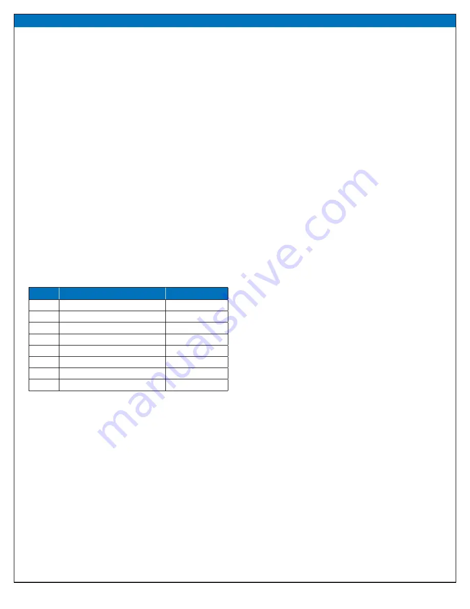
Table 4. J11 Pin Description
J11
Pin Description
Schematic Net Name
1
Not connected
N/A
2
Internal 5 V supply
V5V0
3
Logic supply
Vlogic
4
Internal 3.3 V supply
V3V3
5
Ground
GND
6
Non-inverting differential input
IN_D+
7
Ground
GND
8
Inverting differential input
IN_D-