


QUICK START GUIDE
EPC – THE LEADER IN GaN TECHNOLOGY |
| COPYRIGHT 2019 | | 3
EPC9034
Figure 2: Buck configuration
Figure 3: Boost configuration
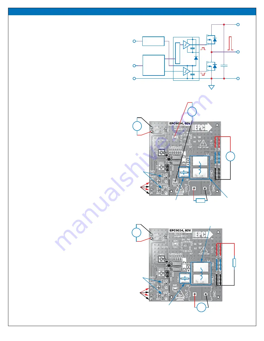
Figure 1: Block diagram of EPC9034 development board
7.5 – 12 V
DC
32 V
DCmax
V
DD
supply
(Note polarity)
V
Main
supply
(Note polarity)
Output Capacitor
Output Inductor
Main voltage measurement
(HIGH VOLTAGE!)
DC load
Dead-time adjust
Control
signal
inputs
+
+
V
Boost Converter configuration
Warning: Never operate the boost converter mode without a load
as the output voltage can increase beyond the maximum ratings.
1. The inductor (L
1
) and input capacitors (labeled as C
out
) can
either be soldered onto the board, as shown in figure 3, or
provided off board. Anti-parallel diodes can also be installed
using the additional pads on the right side of the EPC2021
FETs.
2. With power off, connect the input power supply bus to V
OUT
(J9, Pin-1) and ground / return to GND (J9, Pin-2), or externally
across the capacitor if the inductor L
1
and C
out
are provided
externally. Connect the output voltage (labeled as V
IN
, J5, J6)
to your circuit as required, e.g., resistive load.
3. With power off, connect the gate drive supply to V
DD
(J1,
Pin-1) and ground return to GND (J1, Pin-2 indicated on the
bottom side of the board).
4. With power off, connect the input PWM control signal to
PWM1 (J2, Pin-1) and ground return to any of GND J2 pins
indicated on the bottom side of the board. Note that the
bottom FET gate drive signal is inverted with regard to
PWM1. It is also possible to use separate input PWM signals
by removing R2 and R17 and installing 0 Ω jumpers for R14
and R16.
5. Turn on the gate drive supply – make sure the supply is
between 7.5 V and 12 V.
6. Turn on the controller / PWM input source.
7. Making sure the output is not open circuit, and the input
supply voltage is initially 0 V, turn on the power and slowly
increase the voltage to the required value (do not exceed
the absolute maximum voltage). Probe switching node to
see switching operation.
8. Once operational, adjust the PWM control, bus voltage, and
load within the operating range and observe the output
switching behavior, efficiency and other parameters.
Observe device temperature for operational limits.
9. For shutdown, please follow steps in reverse.
7.5 – 12 V
DC
V
DD
supply
(Note polarity)
Input Capacitor
Input Inductor
Dead-time adjust
Control
signal
inputs
+
32 V
DCmax
DC load
V
Main
supply
(Note polarity)
+
Lev
el shif
t
V
DD
V
IN
Q
1
Q
2
C
Bypass
PWM
GND
Gate drive
regulator
Gate driver
Output
PGND
Logic and
dead-time
adjust


