background image

PCI-82x Series Cards 

Multifunction Boards


User  Manual,  Ver.  1.5,  Jan.  2017,  PMH-024-15,  Page:  38 


  Step 2: 

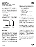
Confirm the PCI-822/826 Series card has 

been successfully installed in the Host system. Note 

that the device numbers start from 0.


Step 3: 

Click the

 “TEST”

 button to start the test.


Step 4: 

Get DIO function test result. 


1.


Click the 

“Digital Output”

 tab. 

2.


Select the 

“Port0”

 from the 

“Port Number”

 drop-down options. 

3.


Check 

channels 0, 2, 4 and 6


Содержание PCI-82x Series

Страница 1: ...ight to change this manual at any time without notice The information furnished by ICP DAS is believed to be accurate and reliable However no responsibility is assumed by ICP DAS for its use nor for a...

Страница 2: ...4 JP4 Digital I O Mode 12 2 2 5 JP8 Digital Input Pull high low 13 2 3 CARD ID SWITCH 14 2 4 BLOCK DIAGRAM 15 2 5 ANALOG INPUT SIGNAL CONNECTIONS 16 2 6 PIN ASSIGNMENTS 21 3 HARDWARE INSTALLATION 22 4...

Страница 3: ...ing Configuration 48 6 5 2 Write the AI Software Trigger 50 6 5 3 Read the FIFO Data 50 6 5 4 Read Write AI Pacer Sampling Rate 50 6 5 5 Read Write MagicScan Counter Value 51 6 5 6 Write AI Pacer Conf...

Страница 4: ...OH 72 A1 5 Analog Input Functions 73 PCI82X_PollingAI 73 PCI82X_PollingAIH 74 PCI82X_StartAI 75 PCI82X_StartAIScan 76 PCI82X_GetAIBuffer 78 PCI82X_GetAIBufferH 78 PCI82X_StopAI 79 A2 DAUGHTERBOARDS 80...

Страница 5: ...Product Page for the PCI 826LU http www icpdas com root product solutions pc_based_io_board pci pci 826lu html Product Page for the PCI 822LU http www icpdas com root product solutions pc_based_io_bo...

Страница 6: ...826 Series cards contain an embedded Card ID switch and onboard pull high pull low resistors for the Digital Input meaning that a unique ID number can be set for each card so that can each card can be...

Страница 7: ...PCI 822LU One 16 bit A D converter with a maximum sample rate of 250 kSamples second PCI 826LU 32 single ended or 16 differential programmable input channels PCI 822LU PCI 826LU Three different A D tr...

Страница 8: ...0 000 M 4pF Trigger Modes Software Pacer Data Transfer Polling Interrupt Accuracy 0 1 of FSR 1 LSB 25 C 10 V 0 05 of FSR 1 LSB 25 C 10 V Input Range Gain 1 2 4 8 Bipolar V 10 5 2 5 1 25 Zero Drift 15...

Страница 9: ...Bus Type 3 3 V 5 V Universal PCI 32 bit Data Bus 16 bit Card ID Yes 4 bit I O Connector Female DB37 x 1 20 pin box header x 2 Dimensions L x W x D 169 mm x 105 mm x 22 mm Power Consumption 1 A 5 V ma...

Страница 10: ...alog Input Type Configuration Refer to Section 2 2 1 JP6 JP7 Analog Output Range Configuration Refer to Section 2 2 2 JP3 JP5 Analog Output Type Configuration Refer to Section 2 2 3 JP4 Digital Input...

Страница 11: ...onfigure single ended input connect pin1 to pin 3 and pin 2 to pin 4 as illustrated in the diagram below The default configuration is single ended Jumper Single ended Input Default Differential Input...

Страница 12: ...e the Digital Input Output mode as either Jumper Selectable or Software Programmable Mode Connecting pins 1 and 2 of DIO S0 sets the DI O mode to Jumper Selectable Mode while connecting pins 2 and 3 s...

Страница 13: ...S0 is Jumper Selectable Mode DI Default DO DIO S1 Port A DIO S2 Port B 1 2 3 1 2 3 2 2 5 JP8 Digital Input Pull high low Jumper JP8 is used to set the Digital Input to either Pull high or Pull low wh...

Страница 14: ...ormat For more detailed information regarding the positions of the SW1 DIP Switch for the different Card ID settings refer to the table below Default Settings Card ID Hex 1 ID0 2 ID1 3 ID2 4 ID3 0x0 O...

Страница 15: ...ck Diagram The following is an illustration of the System Function Block for PCI 822 826 Series cards PCI Bus D I D O Timer A D Buffer A D Converter A D Trigger Logic Multiplexers Gain Amp Scale Adj P...

Страница 16: ...or floating source Analog Input signals Important Note For the method illustrated in Figure 2 5 4 the maximum allowable common mode voltage between the Analog Input source and the AGND pin is 70Vp p s...

Страница 17: ...e 17 Figure 2 5 1 Connecting to a grounded source input correct method A D CH0 HI A D CHn HI A D CHn LO A GND n A D CH0 LO Es 1 Es n S S PCI 822 826 Figure 2 5 2 Connecting to a ground loop input inco...

Страница 18: ...er CAUTION The maximum allowable common mode voltage between the Analog Input source and the A GND pin for the connection shown in Figure 2 5 4 is 70 Vp p Ensure that the input signal is below this va...

Страница 19: ...D Es 1 Es n 100 k 10 M 100 k 10 M PCI 822 826 Figure 2 5 6 Connecting to a 4 20 mA Source AI CHn AGND R Shunt Resistor Example A 20 mA source current through a 125 resistor e g 125 0 1 DIP Resistors b...

Страница 20: ...17 PMH 024 15 Page 20 Signal Shielding The signal shielding for the connection methods illustrated in Figures 2 5 1 to 2 5 6 are the same Use a single point connection to the frame ground rather than...

Страница 21: ...an 2017 PMH 024 15 Page 21 2 6 Pin Assignments The following is an overview of the pin assignments for PCI 822 826 Series cards CON1 and CON2 relate to the Digital Input and Digital Output connectors...

Страница 22: ...er to Chapter 4 Software Installation Step 2 Configure the Jumpers and the SW1 DIP Switch on the PCI 822 826 Series card depending on the required configuration For more detailed information about the...

Страница 23: ...nction Boards User Manual Ver 1 5 Jan 2017 PMH 024 15 Page 23 Step 3 Correctly shut down and power off your computer and then disconnect the power supply Step 4 Remove the cover from the computer Step...

Страница 24: ...ove the slot cover from the PC Ensure that you do not misplace the screw Step 7 Remove the connector cover from the PCI 822 826 Series card Step 8 Align the contacts of the PCI card with the open slot...

Страница 25: ...rm that the PCI 822 826 series card is correctly mounted in the motherboard Step 10 Replace cover for the computer and then reconnect the power supply and any other cables Step 11 Switch on the power...

Страница 26: ...on CD ROM or can be obtained from the ICP DAS FTP web site Install the appropriate driver for the operating system The location and website addresses for the installation package are indicated below U...

Страница 27: ...16 series board on the list then click the Next button Step 6 When the Select Additional Tasks screen is displayed click the Next button Step 7 When the Download Information screen is displayed click...

Страница 28: ...nel 2 4 x 2 6 x 3 12 x Driver Name Ixpci tar gz CD ROM CD NAPDOS Linux Website http ftp icpdas com pub cd iocard pci napdos linux Installation Procedure For more detailed information about how to inst...

Страница 29: ...e computer For detailed information about the hardware installation of the PCI 822 826 Series board refer to Chapter 3 Hardware Installation Step 2 Power on the computer and complete the Plug and Play...

Страница 30: ...PCI 82x Series Cards Multifunction Boards User Manual Ver 1 5 Jan 2017 PMH 024 15 Page 30 Step 4 Click the Finish button Step 5 Windows pops up Found New Hardware dialog box again...

Страница 31: ...appropriate description for the specific operating system to verify the installation 4 3 1 Accessing Windows Device Manager Windows 95 98 ME Step 1 Either right click the My Computer icon on the deskt...

Страница 32: ...Windows Vista 7 Step 1 Click the Start button and then click Control Panel Step 2 Click the System and Maintenance and then click Device Manager Alternatively Step 1 Click the Start button Step 2 In...

Страница 33: ...tep 1 To display the Start screen icon from the desktop view hover the mouse cursor over the bottom left corner of screen Step 2 Right click the Start screen icon then click Device Manager Alternative...

Страница 34: ...ultifunction Boards User Manual Ver 1 5 Jan 2017 PMH 024 15 Page 34 4 3 2 Check the Installation Check that the PCI 822 826 Series card is correctly listed in the Device Manager as illustrated below I...

Страница 35: ...g is a description of how to configure the wiring in order to perform the Self Test procedures for the Digital Input and Digital Output Refer to the appropriate descriptions for PCI 822 826 Series car...

Страница 36: ...Wiring Preparing the device Before beginning the Self Test procedure ensure that the following items are available A CA 3710 cable Website http www icpdas com products Accessories cable cable_selecti...

Страница 37: ...n18 to the AI0 Pin1 and connect the A GND pin Pin17 to the A GND pin Pin17 5 2 Execute the Test Program After installation the UniDAQ Utility will be located in the default folder C ICPDAS UniDAq Driv...

Страница 38: ...822 826 Series card has been successfully installed in the Host system Note that the device numbers start from 0 Step 3 Click the TEST button to start the test Step 4 Get DIO function test result 1 Cl...

Страница 39: ...D A functions test 1 Click the Analog Output tab 2 In the Voltage Output section select the 0 from the Channel drop down menu 3 Select Bipolar 10 V from the Range drop down menu 4 Enter a voltage valu...

Страница 40: ...Click the Analog Input tab 7 Confirm that the configuration settings are correct 8 Click the Start button to start the test 9 Check that the Analog Input value for Channel 0 is the same as the voltag...

Страница 41: ...PCI 826LU Vendor ID 0x10B5 0xE10B5 Device ID 0x3001 0x3001 Sub Vendor ID 0x2129 0x2129 Sub Device ID 0x0822 0x0826 The following functions are provided for the PCI 822 826 card 1 PCI82x_DriverInit wT...

Страница 42: ...ct all PCI 822 PCI 826 cards first wRetVal PCI82X_DriverInit wTotalBoards printf Threr are d PCI 822 PCI 826 Cards in this PC n wBoards Step2 Save resources of all PCI 822 PCI 826 cards installed in t...

Страница 43: ...the status of the DI O Jumper and Card ID Sets the configuration for Port A and Port B 2 D A 0h Reads the D A Data Writes the D A Data 4h Reads the D A control settings Configures the D A control sett...

Страница 44: ...rt can be read written by accessing its data register The I O ports on PCI 822 826 Series cards are 16 bit 6 3 2 Read Write I O Port Selection Read Write wBase 0 0x0C I O Port Selection Bit 1 0 Data P...

Страница 45: ...3 ID2 ID1 ID0 This register is used to read the Card ID SW1 and the DIO Jumper JP4 settings on the PCI 822 826 Series card The following is an example of how to read the 4 bit Card ID wCardID inportb...

Страница 46: ...D A converter provide 2 channel Analog Output Refer to Section 6 4 2 below for details of how to select the D A channel before writing data to the D A converter 6 4 2 Read Write Analog Output Channel...

Страница 47: ...e output to the channel The D A channels are allocated as follows CH x 1 Enable the channel CH x 0 Disable the channel The following is an example of how to enable the Analog Output Channel Set the AO...

Страница 48: ...ng mode software trigger The configuration parameters include the Gain code the Mode single ended or differential and the channel number Clearing the FIFO Bit F Write a value of 1 to F0 to clear the F...

Страница 49: ...as indicated below M3 M2 M1 M0 M5 M4 0 1 1 0 1 1 0 0 0 0 SE Ch0 SE Ch16 DIFF Ch0 0 0 0 1 SE Ch1 SE Ch17 DIFF Ch1 0 0 1 0 SE Ch2 SE Ch18 DIFF Ch2 0 0 1 1 SE Ch3 SE Ch19 DIFF Ch3 0 1 0 0 SE Ch4 SE Ch20...

Страница 50: ...5 4 Read Write AI Pacer Sampling Rate Read Write wBase 0x8 Read Write the AI Pacer Sampling Rate Bit F E D C B A 9 8 7 6 5 4 3 2 1 0 Data CF CE CD CC CB CA C9 C8 C7 C6 C5 C4 C3 C2 C1 C0 This register...

Страница 51: ...uration parameters include the Gain code the Mode single ended or differential and the channel number Clearing the FIFO Bit F Write a value of 1 to F0 to clear the FIFO Data The status of the FIFO wil...

Страница 52: ...ential Analog Input Selection Bits 4 and 5 are used to configure the control Pacer mode for the Analog Input channels as indicated below M5 M4 Analog Input 0 0 x 0 1 Single ended Input Channel 0 15 1...

Страница 53: ...15 Page 53 1 0 0 0 SE Ch8 SE Ch24 DIFF Ch8 1 0 0 1 SE Ch9 SE Ch25 DIFF Ch9 1 0 1 0 SE Ch10 SE Ch26 DIFF Ch10 1 0 1 1 SE Ch11 SE Ch27 DIFF Ch11 1 1 0 0 SE Ch12 SE Ch28 DIFF Ch12 1 1 0 1 SE Ch13 SE Ch29...

Страница 54: ...ferential mode JP1 is set to Single ended mode A0 The ADC is Ready The ADC is Busy FF The FIFO is Full The FIFO isn t Full FH The FIFO is Half Full The FIFO isn t Half Full FE The FIFO is Empty The FI...

Страница 55: ...0 0 1 0 2 MHz 0 0 1 1 1 MHz 0 1 0 0 500 kHz 0 1 0 1 250 kHz 0 1 1 0 125 kHz 0 1 1 1 62 5 kHz Total Number of Channels to be Scanned for MagicScan Bits 3 to 7 Bits 3 to 7 are used to set the total numb...

Страница 56: ...0 Disable Pacer START Bit E 1 Enable Pacer STOP 0 Disable Pacer STOP 6 5 10 Clear the Interrupt and External Trigger Read wBase 0x18 Clear the Interrupt and External Trigger This register is used to...

Страница 57: ...l and then sends the interrupt Bit 2 External Trigger Interrupt 0 Disable 1 Enable 3 Send the interrupt when the FIFO is half full Bit 1 FIFO Half Interrupt 0 Disable 1 Enable 4 Sends the interrupt wh...

Страница 58: ...8030 Set the Software AI Trigger outpw wBase 0x04 0x0000 Disable the Pacer Trigger outpw wBase 0x18 0x4000 Disable the Interrupt outpw wBase 0x1C 0x0000 Set the Gain Channel and clear the FIFO outpw w...

Страница 59: ...al Number of scan Channels to 3 outpw wBase 0x14 0x0001 3 1 3 Set the Frequency to 8 MHz 200 40 KHz outpw wBase 0x08 0xC8 Set the channel number for the first channel to 2 outpw wBase 0x10 0x8032 0 10...

Страница 60: ...he Total Number of Scan Channels to 3 Set the Trigger Edge to Rising and Enable External Trigger Mode outpw wBase 0x14 0x8003 2 3 Set the Frequency to 8 MHz 200 40 KHz outpw wBase 0x08 0xC8 Set the fi...

Страница 61: ...used by IR loss in the cable and or the connector can be eliminated Before beginning calibration ensure that a precise multi meter is available Note that the calibrated values for the Analog Input Out...

Страница 62: ...wing is a demonstration of how to perform the calibration procedure The following pin assignments are used in the calibration process 1 D A Ch0 CON3 pin 18 2 A GND CON3 pin 1 3 D A Ch1 CON3 pin 36 4 A...

Страница 63: ...e for CH0 is 0 V 22 1 Enter the D A data 2 Click the A0 12 button 3 Repeat items 1 and 2 until the D A output voltage for CH0 is 5 V 8 1 Enter the D A data 2 Click the A0 3 button 3 Repeat items 1 and...

Страница 64: ...lling the function Data values from this parameter is retrieved after calling the function Input Yes No Output No Yes Input Output Yes Yes A1 1 Error Code Definitions Error Code Error ID Description 0...

Страница 65: ...ries cards installed in the system are detected the resource information will be saved to the library Syntax WORD PCI82X_DriverInit WORD wBoards Parameters wBoardNo Output The number of boards found o...

Страница 66: ...elated to the PCI 822 826 Series cards Syntax WORD PCI82X_GetConfigAddressSpace WORD wBoardNo WORD wBaseAddr WORD wBaseDIO WORD wBaseDA WORD wBaseAD WORD wIrqNo WORD wModeID WORD wCardID Parameters wB...

Страница 67: ...24 15 Page 67 wModeID Output The Model ID number Sub Device ID see Section 6 1 for details 0x822 is PCI 822 0x826 is PCI 826 wCardID Output The Card ID number as configured using DIP Switch SW1 see Se...

Страница 68: ...ecified board Syntax WORD PCI82X_SetDIOMode32 WORD wBoardNo WORD wDirection Parameters wBoardNo Input The board number Base 0 wDirection Input Configures the mode to be used for Digital I O ports A an...

Страница 69: ...specified board in 16 bit integer format Syntax WORD PCI82X_WriteDO WORD wBoardNo WORD wPortNo WORD wValue Parameters wBoardNo Input The board number Base 0 wPortNo Input The Port number where 0 denot...

Страница 70: ...cified board in 16 bit integer format Syntax WORD PCI82X_ReadDI WORD wBoardNo WORD wPortNo WORD wValue Parameters wBoardNo Input The board number Base 0 wPortNo Input The Port number to be read where...

Страница 71: ...at format Syntax WORD PCI82X_WriteAO WORD wBoardNo WORD wChannel WORD wConfig float fValue Parameters wBoardNo Input The board number Base 0 wChannel Input The D A channel number wConfig Input Configu...

Страница 72: ...specific D A channel on a specified board in 16 bit integer format Syntax WORD PCI82X_WriteAO WORD wBoardNo WORD wChannel WORD wValue Parameters wBoardNo Input The board number Base 0 wChannel Input T...

Страница 73: ...dNo WORD wChannel WORD wConfigCode DWORD dwDataCount float fValue Parameters wBoardNo Input The board number Base 0 wChannel Input The A D channel number wConfigCode Input Configures the voltage range...

Страница 74: ...nnel WORD wConfigCode DWORD dwDataCount WORD wValue Parameters wBoardNo Input The board number Base 0 wChannel Input The A D channel number wConfigCode Input Configures the voltage range for the Analo...

Страница 75: ...Refer to the PCI82X_StopAI function for details of how to stop the pacer trigger operation Syntax WORD PCI82X_StartAI WORD wBoardNo WORD wChannel WORD wConfig float fSamplingRate DWORD dwDataCount Pa...

Страница 76: ...e PCI82X_StopAI function for details of how to stop the MagicScan operation Syntax WORD PCI82X_StartAIScan WORD wBoardNo WORD wChannels WORD wChannelList WORD wConfigList float fSamplingRate DWORD dwD...

Страница 77: ...nnel to be scanned is AI Channel 5 wChannelList 2 3 The third channel to be scanned is AI Channel 3 wConfigList 0 2 The input range for the first channel is 2 5 V wConfigList 1 0 The input range for t...

Страница 78: ...float fValue Parameters wBoardNo Input The Board number Base 0 dwDataCount Input The Analog Input data value fValue Output An array containing the A D data received from the Analog Input channels in...

Страница 79: ...t An array containing the A D data received from the Analog Input channels in 16 bit integer format Returns Refer to Appendix A1 1 Error Code Definitions PCI82X_StopAI This function is used to stop al...

Страница 80: ...terboards DB 37 The DB 37 is a general purpose daughterboard for devices that include 37 pin D sub connectors and is designed for easy wiring DN 37 The DN 37 is a general purpose daughterboard for dev...

Страница 81: ...nal optocoupler with a resistor to allow current sensing The DB 16P can be used to sense DC signals from TTL levels up to 24 V or can be used to sense a wide range of AC signals This board can also be...

Страница 82: ...n industrial type terminal block The Relay channels are powered by applying a 5 V signal to the appropriate channel via a 20 pin flat cable connector The DB 16R includes 16 LEDs one for each Relay cha...

Отзывы: