background image

40

II. FEATURES AND FUNCTIONS

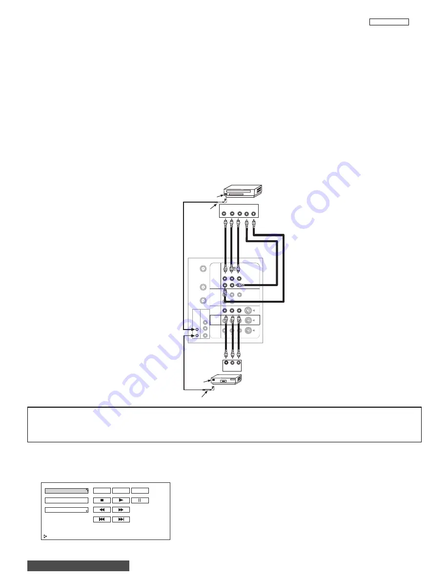
5.0 CONNECTING AV NETWORK

Your Hitachi LCD TV is equipped with an AV Network feature.  This feature helps to control your external Audio/Video equipment
(VCR, Set Top Box, DVD, etc.).  Once this is setup, it allows your IR Mouse connector to control your equipment using your Hitachi
TV Remote Control.  You can use your Hitachi remote control to control the Audio/Video equipment command without the equip-
ment’s remote control.

The television rear panel has 2 IR BLASTER jacks.  Each IR Mouse cable can connect up to 2 external Audio/Video components.
Therefore, you can connect the television with up to four components and control them with the TV remote control.  Please see the
following example of an AV Network setup between your Hitachi LCD TV and external Audio/Video equipment (VCR and DVD
Player).

CONNECTING EXTERNAL AUDIO/VIDEO COMPONENTS TO IR BLASTER FOR AV NETWORK

1.

Connect your external Audio/Video components to the Rear Panel jacks as shown on page 27.

2.

Connect the IR Mouse cable to the IR BLASTER input of the television’s rear panel.

3.

Place the IR mouse in front of the infrared sensor of the external components you wish to control.

NOTES:

1. The rear panel has two IR BLASTER inputs which can control up to a total of four external components.
2. The IR Mouse must be placed in front of the external components IR sensor for the AV Network to work.
3. The correct codes must be entered for each of the Audio/Video components for the AV Network to function 

properly (see page 42).

CENTER

IN

 P

B

P

R

DVI-HDTV

PR

P

R

VIDEO

R

R

(MONO)/L VIDEO

INPUT 3

DVD Player

IR
Sensor

IR
Mouse

VCR

R       L       V

OUTPUT

IR
Sensor

OUTPUT

P

R

/C

R

P

B

/C

B

Y      L       R

R

IR
Mouse

S-VIDEO

ANT A

TO
CONVERTER

ANT B

L

IR
BLASTER

AUDIO
TO HI-FI

R

S-VIDEO

S-VIDEO

Y/VIDEO

R

(MONO)/L

R

(MONO)/L

R

L

VIDEO

INPUT 1

INPUT 2

INPUT 4

MONITOR

OUT

AUDIO

AUDIO

 PB

PR

Y

R

(MONO)/L

4.

Press the A/V NET button on the remote control.  Use THUMB STICK 

or 

to highlight the component you wish to set up.

Use THUMB STICK 

to enter component’s “SOFT KEY” control button.  The AV Network Setup Wizard will automatically start

upon the very first use.  You can access the Setup Menu Wizard again in the future by pressing the INFO button when the
desired equipment is highlighted.

Photo MC

Cable Box

DVD

Move

POWER

MENU

MORE

BACK TO ADJUSTMENTS

LC37/LC37F

Содержание 50V500 - UltraVision Digital - 50" Rear Projection TV

Страница 1: ...NTSC LC37 Chassis LC37F Chassis R C CLU 5729TSI CAUTION Before servicing this chassis it is important that the service technician read the Product Safety Notices in this service manual SAFETY NOTICE USE ISOLATION TRANSFORMER WHEN SERVICING Components having special safety characteristics are identified by a on the parts list in this Service Data and its supplements and bulletins Before servicing t...

Страница 2: ...ician must thoroughly test the unit to be certain that it is completely safe to operate without danger of electrical shock and be sure that no protective device built into the receiver by the manufacturer has become defective or inadvertently defeated during servicing Therefore the following checks should be performed for the con tinued protection of the customer and service technician Leakage Cur...

Страница 3: ...cians it is not meant for the casual do it yourselfer Qualified technicians have the necessary test equipment and tools and have been trained to properly and safely repair complex prod ucts such as those covered by this manual Improperly per formed repairs can adversely affect the safety and reliability of the product and may void warranty Consumers should not risk trying to do the necessary repai...

Страница 4: ...lectrostatically Sensitive ES Devices Some semiconductor solid state devices can be damaged easily by static electricity Such components commonly are called Electrostatically Sensitive ES Devices Examples of typical ES devices are integrated circuits and some field effect transistors and semiconductor chip components The following techniques should be used to help reduce the incidence of component...

Страница 5: ...miliar round hole use the standard technique as outlined in paragraphs 5 and 6 above Removal 1 Desolder and straighten each IC lead in one operation by gent ly prying up on the lead with the soldering iron tip as the solder melts 2 Draw away the melted solder with an anti static suction type sol der removal device or with solder braid before removing the IC Replacement 1 Carefully insert the repla...

Страница 6: ...ound the IC pin Solder the IC connection 4 Route the jumper wire along the path of the cut away copper pattern and let it overlap the previously scraped end of the good copper pattern Solder the overlapped area and clip off any excess jumper wire At Other Connections Use the following technique to repair defective copper pattern at connections other than IC Pins This technique involves the instal ...

Страница 7: ...pads with tweezers or with a miniature alligator clip and apply heat to the pad area with a 30 watt iron until solder flows Do not apply heat for more than 3 seconds How to Replace Flat lC Required Tools Soldering iron iron wire or small awl De solder braids Magnifier 1 Remove the solder from all of the pins of a Flat lC by using a de solder braid 2 Put the iron wire under the pins of the Flat lC ...

Страница 8: ...e complies with Part 15 of the FCC Rules Operation is subject to the following two conditions 1 this device may not cause harmful interference and 2 this device must accept any interference received including interference that may cause undesired operation For questions regarding this declaration contact Hitachi America LTD Home Electronics Division 900 Hitachi Way Chula Vista CA 91914 Tel 1 800 4...

Страница 9: ... Connecting AV Network 40 5 1 AV Network Setup Wizard 41 5 2 AV Network Codes 42 5 3 How To Use AV Network 43 5 4 How To Use The Aspect Mode 48 III ASSEMBLED P W B ADJUSTMENT 49 1 Memory Initialization 49 Table 1 I2 C Parameter List 61 Table 2 Factory Reset 88 2 Factory Reset 50 3 Raster Position Adjustment 51 3 1 Mechanical Raster Position Adjustment 51 3 1 1 Geometry Specifications 51 3 1 2 Adju...

Страница 10: ...t Blcok Diagram 94 V TROUBLE SHOOTING FLOWCHART 95 VI DC VOLTAGE 96 VII WAVEFORMS 108 VIII REPLACEMENT PARTS LIST 114 IX EXPLODED VIEW 138 X PRINTED CIRCUIT BOARD 148 XI CONNECTION DIAGRAM 160 XII BLOCK DIAGRAM 161 XIII BASIC CIRCUIT DIAGRAM 162 XIV FINAL WIRING 175 XV MAJOR ICs and UNITS 179 ...

Страница 11: ...ol up to 4 components with one remote 2 IR Mouse cables included Full Set of Input Jacks including S VIDEO COMPONENT VIDEO Y PB PR Inputs Power Input AC 120V 60Hz Stand by Power 0 6W Power Consumption Pmax 172W Pave 158W Antenna input impedance 75 Ohm Channel coverage 181ch VHF Band 2 13 UHF Band 14 69 CATV Mid Band A 5 A 1 A I Super Band J W Hyper Band W 1 W 28 Ultra Band W 29 W 84 Video 1 0Vp p ...

Страница 12: ...12 LC37 LC37F I SPECIFICATION BACK TO ADJUSTMENTS ...

Страница 13: ...m 3 White Balance HIGH 14 700K 23MPCD X 0 260 0 01 Y 0 280 0 01 MEDIUM 7500K 0MPCD X 0 301 0 02 Y 0 311 0 02 STANDARD 6500K 0MPCD X 0 313 0 02 Y 0 329 0 02 Black White 5400K 0MPCD X 0 334 0 02 Y 0 343 0 02 at screen center TYP MIN 370 cd m2 240 cd m2 257 cd m2 166 cd m2 BACK TO ADJUSTMENTS LC37 LC37F ...

Страница 14: ...14 LC37 LC37F I SPECIFICATION BACK TO ADJUSTMENTS ...

Страница 15: ...15 LC37 LC37F I SPECIFICATION BACK TO ADJUSTMENTS ...

Страница 16: ...16 LC37 LC37F I SPECIFICATION BACK TO ADJUSTMENTS ...

Страница 17: ...17 LC37 LC37F I SPECIFICATION BACK TO ADJUSTMENTS ...

Страница 18: ... 56 75 16 9 Standard 4x3 16x9 16 9 Standard 1386 dots 788 dots 1386 dots 788 dots 4 3 Standard 4x3 4 3 Standard 16x9 998 dots 95 998 dots 95 100 110 120 130 140 150 160 170 180 0 10 20 30 40 50 60 70 80 90 100 4 3 Expanded Mode Horizontal Position Horizontal Expansion Ratio 113 162 4 3 Expanded 113 162 162 4 3 Standard 100 I SPECIFICATION 6 1 3 Aspect Mode Resolution BACK TO ADJUSTMENTS ...

Страница 19: ...ep 720p Video 1 DVI 1080i 16x9 0 10 Step _ _ _ _ 480i 480p 4x3 16x9 0 10 Step 0 10 Step 10 Step 10 Step 720p YPBPR 1080i 16x9 0 10 Step _ _ _ _ Video 2 Video NTSC 4x3 16x9 0 10 Step 0 10 Step 10 Step 10 Step Video 3 Video S Video NTSC 4x3 16x9 0 10 Step 0 10 Step 10 Step 10 Step Video 4 Video S Video NTSC 4x3 16x9 0 10 Step 0 10 Step 10 Step 10 Step Video 5 Video S Video NTSC 4x3 16x9 0 10 Step 0 ...

Страница 20: ...20 LC37 LC37F I SPECIFICATION BACK TO ADJUSTMENTS ...

Страница 21: ...6x9 16x9 16x9 16x9 16x9 228 dots 788 dots 788 dots 95 4x3 4x3 4x3 4x3 4x3 4x3 788 dots 788 dots 262 dots 788 dots 249 dots 262 dots 788 dots 4x3 4x3 4x3 4x3 4x3 262 dots 262 dots 1386 dots 1042 dots 344 dots 1386 dots 304 dots 1386 dots 455 dots 332 dots 344 dots 693 dots 4x3 I SPECIFICATION 6 2 2 PIP Mode Resolution BACK TO ADJUSTMENTS ...

Страница 22: ...it is set to a level 30 or less the volume level will be at the level it was set when the TV is turned ON FRONT INPUT JACKS INPUT 5 Use these audio video jacks for a quick hook up from a camcorder or VCR to instantly view your favorite show or new recording Press the INPUT EXIT button on the front control panel until VIDEO 5 appears in the top right corner of the TV screen If you have mono sound i...

Страница 23: ... DOWN LIGHT ON BLINKING LIGHT ON BLINKING LIGHT ON SLOWLY BLINKING INDICATOR INDICATION MEANING ACTION LAMP LED TEMP LED POWER Need to replace if LAMP still does not light by Power On again Check assembly condition of LAMP UNIT NOTES 1 2 If the LAMP TEMP and POWER LED are blinking in the order below the television is warming up POWER TEMP LAMP IMPORTANT NOTES 1 A small number of missing discolored...

Страница 24: ...wing examples NOTE 1 Completely insert connection cord plugs when connecting to front panel jacks If you do not the played back picture may be abnormal 2 If you have a S VHS VCR use the S INPUT cable in place of the standard video cable 3 If you have a mono VCR insert the audio cable into the left audio jack of your TV INPUT 5 S VIDEO VIDEO AUDIO L MONO R INPUT 5 S VIDEO VIDEO AUDIO L MONO R ...

Страница 25: ... VIDEO Output for high quality video output AUDIO TO HI FI Output These jacks provide variable audio output to a separate stereo amplifier With this connection the audio to the stereo can be controlled by the television s main volume CENTER IN Input This jack is for stereo amplifiers with center signal capability This feature allows the TV speakers to be used as a center speaker The TV must be set...

Страница 26: ...ts 5 To ensure no copyright infringement the MONITOR OUT output will be abnormal when using the Y PBPR jacks 6 Input 2 Y VIDEO can be used for composite video and component video input IR Blaster This jack provides IR output to your external components VCR Cable box DVD player etc With this connection your external components can automatically be controlled by the AV Net feature This connection wi...

Страница 27: ...R BLASTER CONNECT TO IR BLASTER IR Sensor IR Sensor PB PR CENTER IN PB PR DVI HDTV CENTER OUTPUT L R INPUT OUTPUT INPUT ANT A TO CONVERTER ANT B L Y R MONO L IR BLASTER AUDIO TO HI FI R S VIDEO S VIDEO S VIDEO Y VIDEO R MONO L R MONO L VIDEO R MONO L VIDEO R L VIDEO INPUT 1 INPUT 2 INPUT 3 INPUT 4 MONITOR OUT AUDIO AUDIO AUDIO TYPICAL FULL FEATURE SETUP NOTES 1 Connect only 1 component to each inp...

Страница 28: ...ct only 1 component VCR DVD player camcorder etc to each input jack COMPONENT Y PBPR Input 1 2 connections are provided for high performance components such as DVD players and set top boxes Use these connections in place of the standard video connection if your device has this feature Input 2 accepts both composite and component video signals Your component outputs may be labeled Y B Y and R Y In ...

Страница 29: ... Industries Alliance at www eiae org in the U S or Electronic Product Stewardship Canada at www epsc ca in Canada CAUTION A LAMP indicator will light when lamp becomes hot Unplug product s power cord from the AC outlet and allow lamp to cool for at least 30 45 minutes If LAMP indicator is still lit check the lamp unit assembly NOTES Contact your Hitachi dealer for a new lamp unit Using other lamps...

Страница 30: ...OOL BEFORE PROCEEDING WITH LAMP REMOVAL FRONT COVER PUSH PULL LAMP COMPARTMENT 2 Remove the front cover from the TV set This is held by a snap on Pull the front cover outwards until the quick snap on disengages NOTE The lamp in this product contains Mercury Dispose of properly in accordance with applicable environmental laws For Recycling and Disposal information contact your respective government...

Страница 31: ... DO NOT PUT YOUR HAND IN THE LAMP STORAGE AREA AFTER THE LAMP UNIT IS REMOVED YOU MAY GET BURNED 5 Replace with the new lamp Place the removed lamp into the empty box of the replacement lamp Do not touch the front glass of the new lamp or its receptacle This may shorten the life of the lamp and reduce the picture quality Push the lamp unit back to its original position Tighten the screws firmly on...

Страница 32: ...and turn on the main power switch 120V PUSH POWER NOTE The lamp in this product contains Mercury Dispose of properly in accordance with applicable environmental laws For Recycling and Disposal information contact your respective governmental agencies or the Electronic Industries Alliance at www eiae org in the U S or Electronic Product Stewardship Canada at www epsc ca in Canada II FEATURES AND FU...

Страница 33: ...ternal Speakers Select TV s internal speakers On Off or use as center speaker Auto Noise Cancel Eliminates the noise between stations Perfect Volume Adjust volume in fixed setting Loudness Adjust Loudness Mode Choose the picture format aspect ratio Ant A View edit Channel ID Scan and Lock settings in antenna A Ant B View edit Channel ID Scan and Lock settings in antenna B Change Access Code Change...

Страница 34: ...B STICK SELECT THUMB STICK Color Brightness Contrast Picture Mode Video Move SEL Select Color Temperature Sharpness Tint Contrast Mode Black Enhancement 100 50 50 50 High Locks Chan Manager Aspect Audio Video Move SEL Sel SEL Select Day Night Setup Reset Video Settings ANT A B High Dynamic Picture Mode Day Night Return Next Prev Function Day Night Reset Reset the video menu settings on current inp...

Страница 35: ... selected and adjusted in the same manner 2 It may be necessary to adjust TINT to obtain optimum picture quality when using the COMPONENT VIDEO Y PBPR input jacks Use this function to adjust flesh tones so they appear natural Tint Use this function to adjust the amount of fine detail in the picture Sharpness function will be disabled when Noise Reduction is On Sharpness Use this function to choose...

Страница 36: ... o m e n u S e t t i n g s o n t h i s i n p u t t o t h e o r i g i n a l f a c t o r y s e t t i n g s R e s e t THUMB STICK SELECT THUMB STICK Color Brightness Contrast Picture Mode Video Move SEL Select Color Temperature Sharpness Tint Contrast Mode Black Enhancement 100 50 50 50 High Day Night Reset Video Settings ANT A B High Dynamic Noise Reduction Auto Color Color Decoding Video Move SEL S...

Страница 37: ...ames or still pictures per second instead of 30 frames or 60 fields like video When film is transferred to video for television viewing the disparity between the two frame rates must be reconciled This involves a process known as 3 2 pulldown When Auto Movie Mode is turned On from the Video menu your Hitachi LCD TV will activate the circuitry for this special feature to improve video performance w...

Страница 38: ...SEL Return Channel Source Antenna Cable 1 Cable 2 Auto Channel Scan Start THUMB STICK SELECT THUMB STICK Move SEL Select Channel Source Antenna Cable 1 Cable 2 Auto Channel Scan Start Ant B Chan Manager Move SEL Select Ant A Channel List Chan Manager Ant A Channel List Chan Manager Ant A RECEPTION BAND CATV 1 OR CATV 2 AIR VHF 2 13ch UHF 14 69ch CATV CHANNEL VHF 2 13 Mid band A 1 A 5 A 1 Super ban...

Страница 39: ...epeat Auto Channel Scan for the second antenna input Remember to select the correct Antenna Cable mode before using Auto Channel Scan See Channel Manager Scan to add or to erase additional channels Auto Channel Scan THUMB STICK SELECT THUMB STICK SEL Cancel Cancel Scanning Channel Number 66 Move SEL Select Channel Source Auto Channel Scan Start Chan Manager Ant A Channel List Antenna Cable 1 Cable...

Страница 40: ...ision s rear panel 3 Place the IR mouse in front of the infrared sensor of the external components you wish to control NOTES 1 The rear panel has two IR BLASTER inputs which can control up to a total of four external components 2 The IR Mouse must be placed in front of the external components IR sensor for the AV Network to work 3 The correct codes must be entered for each of the Audio Video compo...

Страница 41: ...T SETTING LIST Device Code Video Audio DVD 0672 INPUT 1 Using TV VCR Not Setup Not Setup CBL Not Setup Not Setup STB Not Setup Not Setup PVR Not Setup Not Setup AVR Not Setup Not Setup Custom Not Setup Not Setup EXIT HITACHI AV NET SET UP DVD Device Code 0 6 7 2 Enter code 9999 to uninstall Video Input Input 1 Audio Input Using TV Transmission Test POWER PLAY CH UP BACK OK EXIT Move SEL Select Set...

Страница 42: ...ncepts 0503 Yamaha 0490 0545 0539 Zenith 0591 0503 CABLE BRAND CODE ABC 0003 0008 0014 0017 Americast 0899 Bell Howel 0014 Bell South 0899 Director 0476 General Instrument 0003 0476 0276 0810 GoldStar 0144 Hamlin 0009 0273 Jerrold 0476 0003 0276 0012 0014 0810 Memorex 0000 Motorola 0476 1106 0276 0810 Pace 0237 Panasonic 0107 0000 Philips 0305 0317 Pioneer 0144 0533 0877 1877 Pulsar 0000 Quasar 00...

Страница 43: ...pment soft keys The equipment list will scroll up or down Photo MC Cable Box DVD Move POWER MENU MORE THUMB STICK SELECT THUMB STICK INFO Device Setting Photo MC Cable Box DVD Move POWER MENU MORE SEL Previous Page 1 2 3 4 5 6 7 0 9 8 MORE Move POWER INFO Device Setting CH CH MENU TV VCR MORE Move POWER SEL Previous Page CH CH MENU TV VCR MORE 1 2 3 4 5 6 7 0 9 8 THUMB STICK SELECT MORE THUMB STIC...

Страница 44: ...10 7 10 6 10 5 10 9 10 10 10 THUMB STICK 1 10 2 10 3 10 4 10 8 10 7 10 6 10 5 10 9 10 10 10 No 7 10 03 04 03 1632x1232 Picture No Date Resolution 1 10 2 10 3 10 4 10 8 10 7 10 6 10 5 10 9 10 10 10 1 10 2 10 3 10 4 10 8 10 7 10 6 10 5 10 9 10 10 10 Jump Slideshow Rotate Please Enter Picture Number 1 10 2 10 3 10 4 10 8 10 7 10 6 10 5 10 9 10 10 10 No 7 10 03 04 03 1632x1232 Picture No Date Resoluti...

Страница 45: ...nterval time from 5 10 and 30 seconds Each press will change interval time from the three mentioned choices Press SELECT to stop on a chosen picture of the slideshow After 30 seconds the slideshow will resume or press SELECT again to continue the slideshow Press EXIT to exit the slideshow NOTES 1 Photo file names modified on a computer should be 8 characters Ex ABCD1234 jpg 1st character letters 2...

Страница 46: ...K POWER CH CH MENU TV VCR INFO GUIDE MORE THUMB STICK Custom Set Top Box Move INFO Device Setting Custom Set Top Box Move INFO Device Setting THUMB STICK SETUP THUMB STICK POWER CH CH MENU INFO GUIDE 1 2 3 4 5 6 7 0 9 8 LAST CH Photo MC Cable Box DVD Move POWER MENU MORE INFO Device Setting THUMB STICK C See Page 47 B HITACHI AV NET WIZARD Learning Use this wizard to manually learn or modify your ...

Страница 47: ...AV NET WIZARD Learning Transfer was successfull Press OK to continue BACK OK OK HITACHI AV NET WIZARD Learning Select another DVD2 softkey to learn TV Softkeys Done Continue POWER MENU SELECT EXIT Done HITACHI AV NET WIZARD Learning DVD2 Custom Video Input No Connection Audio Input No Connection Transmission Test POWER PLAY CH UP BACK OK EXIT OK HITACHI AV NET SETTING LIST Device Code Video Audio ...

Страница 48: ... from the center towards the edges of the display area in order to fill it 4 3 Zoom1 Zoom2 Use these aspect modes to zoom in on conventional 4 3 sources 16 9 Standard Use this aspect mode to display 16 9 sources like HDTV and DVD s preserving the original 16 9 aspect ratio 16 9 Zoom Use this aspect mode to zoom 16 9 images 1 NTSC 480i 480p Input 2 480i 480p INPUT 3 720p 1080i INPUT 4 3 INPUT 4 3 E...

Страница 49: ...ly allow you to set these items only when a SDTV or HDTV signal is input to the COMPONENT jacks on the back of the TV 3 Check the OSD according to table on page 61 87 using buttons on the Remote Control to scroll down and cursor right and hold for two seconds to enter the selected device 4 Press the EXIT button to exit I2C ADJUST mode 5 Press the EXIT button button again to EXIT the I2 C menu ADJU...

Страница 50: ...RKS SUB BRIGHT ADJUST DATA BRIGHTNESS DATA NOT INITIALIZE WHITE BALANCE ADJUST DATA G DRV and others NOT INITIALIZE H POSITION ADJUST DATA INITIALIZE NOT INITIALIZE VD POSITION ADJUST DATA INITIALIZE NOT INITIALIZE SUB CONTRAST ADJUST DATA NOT INITIALIZE OSD POSITION SETTING DATA NOT INITIALIZE SETTING DATA FOR EACH DEVICE NOT INITIALIZE BBE EFFECT SETTING DATA NOT INITIALIZE AUDIO AGC SETTING DAT...

Страница 51: ...ION VERTICAL LINE A B 3 TILT VERTICAL LINE J TRAPEZOIDAL DISTORTION HORIZONTAL LINE C D 3 TILT HORIZONTAL LINE K EDGE LINE POSITION VERTICAL E F 6 HORIZONTAL G H 6 CONDITION 1 RECEIVE THE HITACHI CIRCLE PATTERN SIGNAL 2 BRIGHTNESS CONTRAST STANDARD CONDITION CONTRAST MAX OTHER PARAMETERS CENTER POSITION A B C D Parallel Parallel J K E F G H III ASSEMBLED P W B ADJUSTMENT BACK TO ADJUSTMENTS ...

Страница 52: ...XING SCREW FOR TRAPEZOID DISTORTION A 2 ADJUSTMENT SCREW FOR TRAPEZOID DISTORTION B FIXING SCREW FOR TILT C FIXING SCREW FOR VERTICAL RASTER POSITION D FIXING SCREW FOR HORIZONTAL RASTER POSITION C A 1R A 2R B D D C B A 1L A 2L Base plate 3 Base plate 2 Base plate 1 III ASSEMBLED P W B ADJUSTMENT BACK TO ADJUSTMENTS ...

Страница 53: ...5 CONFIRM VERTICAL POSITION 6 IF OUT OF SPEC ADJUST VERTICAL POSITION REFER TO 3 1 4 3 VERTICAL POSITION 7 WHEN STILL OUT OF SPEC ADJUST VERTICAL POSITION BY I C MENU 8 CONFIRM HORIZONTAL POSITION 9 IF OUT OF SPEC ADJUST HORIZONTAL POSITION REFER TO 3 1 4 4 HORIZONTAL POSITION 10 WHEN STILL OUT OF SPEC ADJUST HORIZONTAL POSITION BY I C MENU 2 2 2 III ASSEMBLED P W B ADJUSTMENT 3 1 4 BACK TO ADJUST...

Страница 54: ... specification by mechanical raster position alignment adjust position by I C menu 1 Enter H POSITION service menu and adjust horizontal picture position by using the cursor on the remote contorl 2 Enter V POSITION service menu and adjust vertical picture position by using the cursor on the remote control 2 BACK TO ADJUSTMENTS ...

Страница 55: ...LC37 LC37F 4 0 DISPLAY AREA SPECIFICATIONS III ASSEMBLED P W B ADJUSTMENT BACK TO ADJUSTMENTS H size marker 50V500 0 5 1 0 16mm 60V500A 0 5 1 0 20mm H size marker 50V500 0 5 1 0 16mm 60V500A 0 5 1 0 20mm A ...

Страница 56: ...il Auto Adjusting OSD is disappeared Sample of ADJUST MODE Menu Remarks RGB amplitude adj signal Black White 0 7V 6 0 Sub contrast adjustment Preparation 1 Receive Sub contrast adjustment signal Fig 1 1 Adjustment 1 Select SUB CONTRAST of Service Adj Menu 2 Press for over 2 secondsto perform automatic adjustment When it s completed Auto Adjusting on the screen will be disappeared Fig 1 Full White ...

Страница 57: ...STMENT 1 SIGNAL Internal signal from IC 50 raster signal with one dot black lines 2 Red FLICKER ADJUSTMENT SELECT ADJUST MODE LCD ADJUST V COM with handset You should reduce the flicker by pressing left or right button of handset The adjustment point is the weakest FLICKER position 3 GREEN FLICKER ADJUSTMENT Press SELECT key then the internal signal will be changed from red to green Same procedure...

Страница 58: ...1 ADJUSTMENT PROCEDURE for SERVICE Input signal level luminance level is divided into 32 No 0_No 32 FOR EXAMPLE If customer require to change the white balance of 12th level of white to reddish increase the red value and adjust the white balance of 12th signal level see below I2C MENU LCDADJ GAMMA No 12 STORE THE DATA TO TV SET LCD ADJ G C WRITE_press for several second After this procedure this n...

Страница 59: ...en 1 COLOR UNIFORMITY ADJUSTMENT PROCEDURE Adjustable luminance level is divided in 4 MIN 8 MIDL 20 MIDH 55 and HMAX 82 FOR EXAMPLE If a customer complains about the color uniformity at position 5 on the screen luminance level MIDH increase the BLUE or GREEN or RED value and adjust the color uniformity of position 5 I2C MENU LCDADJ C UNIF MIDH POINT No 5 STORE THE DATA TO TV SET LCD ADJ G C WRITE ...

Страница 60: ...mp holder again 14 0 HIGH TEMPERATURE PROTECTION OPERATION CHECK Adjustment procedure 1 Remove EPF2 connector while the set is on 2 Check that the lamp is turned off and Temp indicator is flash red 3 Turn the set off and attach EPF2 again 4 Remove EPF3 connector while the set is on 5 Check that the lamp is turned off and Temp indicator is flash red 6 Turn the set off and attach EPF3 again 7 Turn t...

Страница 61: ... and Standard data are the offset from High data Data M High Medium 7Fh Data S High Standard 7Fh Data B High B W 7F Black White 17H D07 D0 00 FF 6A High 0CH D18 D8 000 7FF 400 Medium 0FH D18 D8 000 7FF 400 Standard 12H D18 D8 000 7FF 400 R CUTOFF HIGH R CUTOFF MED R CUTOFF STD R CUTOFF B W R SUB BRT CXD3536 000 1023 7FF 1023 steps Medium and Standard data are the offset from High data Data M High ...

Страница 62: ... BM V OSD Vertical Position Bridge Media _ 00 FF 1E AFC CLOCK TEST OFF MEMORY INITIAL I2C OPEN OFF IR BLASTER DIGITAL MODULE FC4 RGB FLA ON 04H D14 0 1 0 Sub mi com LCD ADJUST See Table LCD ADJUST Mode Device Page Sync Frequency Detection Adjustment Mode OSD Adjustment Item Address Adjustment Range HEX Initial Data HEX Adjustment Value HEX Sync Frequency Detection HFRQ N The number of times of Syn...

Страница 63: ... only 00 1F 0A VIDEO ID VIDEO ID Detection Remark VIDEO ID DATA detected by main mi com _ 00 02 IR BLASTER Adjustment Mode OSD Adjustment Item Address Adjustment Range HEX Initial Data HEX Adjustment Value HEX IR BLASTER WAIT _ _ 03 REPEAT IR Blaster Adjustment Refer to IR Blaster doc for Detail Spec _ _ 20 ISF Mode Adjustment Mode OSD Adjustment Item Address Adjustment Range HEX Initial Data HEX ...

Страница 64: ...Fh SIG C 0 1V 0AH D06 D00 00 7F 00h SIDB R 0 SIDB R CXA7005 Red 06h D6 D0 00 SIG C 5 5V 7Fh SIG C 0 1V 0BH D22 D16 00 7F 56h SIDB G 0 SIDB G CXA7005 Green 06h D6 D0 00 SIG C 5 5V 7Fh SIG C 0 1V 0BH D14 D08 00 7F 56h SIDB B 0 SIDB B CXA7005 Blue 06h D6 D0 00 SIG C 5 5V 7Fh SIG C 0 1V 0BH D06 D00 00 7F 56h USR BRT USR BRT CXD3536 2004h D4 D0 CXD3536 2005h D7 D2 000 1024 step 7FF 1023 step 19h D10 D0...

Страница 65: ...A Vertical Aperture Control Gain for Day Mode 0 Correction OFF 7 Correction MAX x0 875 Night Mode is fixed to 0 0AH D7 D5 00 07 05 VAPIN Vertical Aperture Control Invert 0 Correction OFF 1F Correction MAX x0 875 0AH D4 D0 00 1F 03 YPFG Y Peaking Filter Gain Control 0 1 0 8 0 0 F 0 875 0BH D3 D0 00 0F 08 YHC1 TV 00 YHC1 NR TV NR 02 YHC2 NTSC 00 YHC2 NR Y Output High Frequency Coring 0 Coring OFF 1 ...

Страница 66: ...ction 0 OFF 1 40 ns 2 80 ns 3 120 ns ALL 07H D1 D0 03 00 AFCRAN0 Horizontal AFC Switch 0 Normal 1 Narrow ALL 00H D1 00 01 00 FDET 3 Frequency Detection Input Switch 0 480i 1 NTSC 1 480i 2 NTSC 2 D SYNC2 3 HD VD ANT A B NTSC 01H D7 D6 00 03 00 HSEPL 3 ANT A B NTSC 00 HSEPL 4 480i 00 HSEPL 5 480p 00 HSEPL J Horizontal Sync Separation Level Switch 0 20 1 27 2 34 3 40 720p 1080i ANT C 01H D5 D4 00 03 ...

Страница 67: ...e Interpolation 0 OFF 1 ON 01H D19 00 01 00 SHP1 TV 19 19 19 19 SHP1 NR TV NR 08 SHP2 NTSC 13 SHP2 NR NTSC NR 08 SHP4 480i 19 SHP4 NR 480i NR 08 SHP5 480p SHP6 720p SHP7 1080i SHPT NR Sharpness Control Controls Y V H Enhance Gain 480p 720p 1080i NR 02H D04 D00 00 1F 08 HE1 TV 01 HE1 NR TV NR 00 HE2 NTSC 01 H E3 NR NTSC NR 00 HE4 480i 01 HE4 NR 480i NR 00 HE5 480P 01 HEJ 720p 1080i 01 HET NR H Enha...

Страница 68: ...offset for 4 3 Standard 07H D07 D00 00 FF BC BSGOFS Black Stretch Gain Offset ALL 07H D21 D16 00 3F 1F COLORD SDTV NT1 NT2 HD3 HD4 HD6 66 COLORE Color Adj Color CM HDTV NT3 HD2 HD1 HD5 08H D14 D08 00 7F 66 TINTD SDTV NT1 NT2 HD3 HD4 HD6 89 TINTE Tint Adj Tint CM HDTV NT3 HD2 HD1 HD5 08H D07 D00 00 FF 81 HDMODE8 HD1 HD4 00 FLAON Auto signal level adj FLAON 04H D14 0 1 0 Color temp High 1F R C O M C...

Страница 69: ...Sub mi com VS DAT1 VS_DAT1 5 0 CXD3536 20H D21 D16 00 3F 1F VS DAT2 VS_DAT2 5 0 CXD3536 20H D13 D8 00 3F 1F VS DAT3 VS_DAT3 5 0 CXD3536 20H D5 D0 00 3F 1F VS DAT4 VS_DAT4 5 0 CXD3536 21H D21 D16 00 3F 1F VS DAT5 VS_DAT5 5 0 CXD3536 21H D13 D8 00 3F 1F VS DAT6 VS_DAT6 5 0 CXD3536 21H D5 D0 00 3F 1F VS DAT7 VS_DAT7 5 0 CXD3536 22H D21 D16 00 3F 1F VS DAT8 VS_DAT8 5 0 CXD3536 22H D13 D8 00 3F 1F VS D...

Страница 70: ...01 19 01 R R UNIF CXD3536 4000h 26H D15 D08 00 FF _ G G UNIF CXD3536 5000h 26H D07 D00 00 FF _ B B UNIF CXD3536 6000h 27H D07 D00 00 FF _ C UNIF MIDH Sub mi com POINT No C UNIF No 25H D05 D00 01 19 01 R R UNIF CXD3536 4000h 26H D15 D08 00 FF _ G G UNIF CXD3536 5000h 26H D07 D00 00 FF _ B B UNIF CXD3536 6000h 27H D07 D00 00 FF _ C UNIF MAX Sub mi com POINT No C UNIF No 25H D05 D00 01 19 01 R R UNIF...

Страница 71: ...5 0 FFH 128 80H 20 014H SBG Not Use PC 0 255 0 FFH 128 80H 21 015H SBB Not Use PC 0 255 0 FFH 128 80H 22 016H SCR Not Use PC 0 255 0 FFH 168 A8H 23 017H SCG Not Use PC 0 255 0 FFH 168 A8H 24 018H SCB Not Use PC 0 255 0 FFH 168 A8H 25 019H KMOSD OSD Blend Ratio Mode Switch 0 31 0 1FH 17 11H 26 01AH OSDH OSD Horizontal Standard Position 0 255 0 FFH 0 0H 27 01BH OSDV OSD Vertical Standard Position 0 ...

Страница 72: ... 7 0 7H 1 1H 65 041H DMVWHP3 720p 0 7 0 7H 6 6H 66 042H DMVWHP4 VGA 0 7 0 7H 5 5H 67 043H DMVWHP5 SAMSUNG1080i 0 7 0 7H 7 7H 68 044H DMVWHP6 SAMSUNG720P 0 7 0 7H 2 2H 69 045H DSVWHP0 Vertical Write Horizontal Phase 480i 0 7 0 7H 7 7H 70 046H DSVWHP1 DVI Sub 480p 0 7 0 7H 5 5H 71 047H DSVWHP2 1080i 0 7 0 7H 1 1H 72 048H DSVWHP3 720p 0 7 0 7H 6 6H 73 049H DSVWHP4 VGA 0 7 0 7H 5 5H 74 04AH DSVWHP5 SA...

Страница 73: ...0i 0 15 0 FH 2 2H 111 06FH VECOR3 P1 480p 0 15 0 FH 0 0H 112 070H VECOR4 P1 1080i 720p 0 15 0 FH 0 0H 113 071H VECOR5 P1 ANT 3 0 15 0 FH 1 1H 114 072H VECOR6 P1 ANT Video 480i 0 15 0 FH 3 3H 115 073H VECOR7 P1 480p 1080i 720p 0 15 0 FH 15 FH 116 074H VECORPC P1 PC 0 15 0 FH 0 0H 117 075H HECOR0 P2 Horizontal Coring ANT Multi 0 15 0 FH 0 0H 118 076H HECOR1 P2 Video 0 15 0 FH 0 0H 119 077H HECOR2 P2...

Страница 74: ... 480i 0 7 0 7H 4 4H 148 094H SCNRG2 Sub C Frame Noise Reduction Input Gain 4Pix 12Pix ANT Video 480i 480p 1080i 720p 480p 1080i 720p 480p 1080i 720p 0 7 0 7H 4 4H 149 095H MYNRP0 Not Use for PDP ANT Multi 0 7 0 7H 0 0H 150 096H MYNRP1 Video 0 7 0 7H 0 0H 151 097H MYNRP2 480i 0 7 0 7H 0 0H 152 098H MYNRP3 480p 0 7 0 7H 0 0H 153 099H MYNRP4 1080i 720p 0 7 0 7H 0 0H 154 09AH MYNRP5 ANT Video 3 0 7 0 ...

Страница 75: ...7H 7 7H 202 0CAH YCOR7 P0 480p 1080i 720p 0 7 0 7H 7 7H 203 0CBH YVEG0 P1 Not Use for PDP ANT Video 480i Multi 0 15 0 FH 15 FH 204 0CCH YVEG1 P1 480p 0 15 0 FH 4 4H 205 0CDH YVEG2 P1 1080i 720p 0 15 0 FH 15 FH 206 0CEH YVDSBG0 P1 Not Use for PDP ANT Video 480i Multi 0 3 0 3H 0 0H 207 0CFH YVDSBG1 P1 480p 0 3 0 3H 0 0H 208 0D0H YVDSBG2 P1 1080i 720p 0 3 0 3H 3 3H 209 0D1H YVDSBC0 P1 Not Use for PDP...

Страница 76: ...P0 P2 Y G Vertical Enhance ANT Video 480i Multi 0 1 0 1H 0 0H 254 0FEH YVECLP1 P2 480p 1080i 720p 0 1 0 1H 0 0H 255 0FFH YVECLPL0 P2 Y G Vertical Clip Offset Level ANT Video 480i Multi 0 15 0 FH 15 FH 256 100H YVECLPL1 P2 480p 1080i 720p 0 15 0 FH 5 5H 257 101H YVNLP0 P2 Y G Vertical Non Linear Peaking ANT Video 480i Multi 0 63 0 3FH 0 0H 258 102H YVNLP1 P2 480p 1080i 720p 0 63 0 3FH 0 0H 259 103H...

Страница 77: ...20p 0 15 0 FH 9 9H 301 12DH CHDSBG0 ANT Video 480i Multi 0 3 0 3H 0 0H 302 12EH CHDSBG1 B Y B R Y R Horizontal Dynamic Shoot Balance Gain 480p 1080i 720p 0 3 0 3H 0 0H 303 12FH CHDSBC0 ANT Video 480i Multi 0 7 0 7H 0 0H 304 130H CHDSBC1 B Y B R Y R G Horizontal Dynamic Shoot Balance Coring 480p 1080i 720p 0 7 0 7H 0 0H 305 131H CHECLP0 B Y B R Y R Horizontal Enhance ANT Video 480i Multi 0 1 0 1H 0...

Страница 78: ...rizontal Edge Coring ANT Video 480i 0 255 0 FFH 4 4H 345 159H YNIPHECR1 1080i 0 255 0 FFH 4 4H 346 15AH YNIPSBCR Y Slant Difference Coring ANT Video 480i 1080i 0 255 0 FFH 20 14H 347 15BH YNIPV2CR Y Slant Vertical Edge 2 Coring ANT Video 480i 1080i 0 255 0 FFH 20 14H 348 15CH YNIPV1CR Y Slant Vertical Edge 1 Coring ANT Video 480i 1080i 0 255 0 FFH 20 14H 349 15DH YVEGAIN Y Vertical Edge Detection ...

Страница 79: ...FSCB3 P0 1 Not Use DVI Not VGA 0 255 0 FFH 128 80H 381 17DH CLPOFSCR3 P0 1 Not Use DVI Not VGA 0 255 0 FFH 128 80H 382 17EH CLPOFSCB4 P0 1 Not Use DVI VGA 0 255 0 FFH 128 80H 383 17FH CLPOFSCR4 P0 1 Not Use DVI VGA 0 255 0 FFH 128 80H 384 180H CLPOFSCB0 P2 B Y Clamp offset for LCD PDP50î ANT Video 480i 480p 0 255 0 FFH 128 80H 385 181H CLPOFSCR0 P2 R Y Clamp offset for LCD PDP50î ANT Video 480i 48...

Страница 80: ...2 1A6H HUKC4 CbCr Hue Slope 4 127 CbCr 0 255 0 FFH 64 40H 423 1A7H HUCENMC5 0 3 0 3H 3 3H 424 1A8H HUCENLC5 CbCr Hue Center 5 MSB LSB CbCr 0 1023 0 3FFH 941 3ADH 425 1A9H HUWC5 CbCr Hue Width 5 CbCr 0 255 0 FFH 180 B4H 426 1AAH HUCLPC5 CbCr Hue Clip 5 0 128 128 0 255 127 CbCr 0 255 0 FFH 128 80H 427 1ABH HUKC5 CbCr Hue Slope 5 CbCr 0 255 0 FFH 38 26H 428 1ACH HUCENMC6 0 3 0 3H 1 1H 429 1ADH HUCENL...

Страница 81: ...Clip 4 0 128 128 0 255 127 CbCr 0 255 0 FFH 115 73H 462 1CEH SAKC4 CbCr Saturation Slope 4 CbCr 0 255 0 FFH 64 40H 463 1CFH SACENMC5 0 3 0 3H 3 3H 464 1D0H SACENLC5 CbCr Saturation Hue Center 5 MSB LSB CbCr 0 1023 0 3FFH 1004 3ECH 465 1D1H SAWC5 CbCr Saturation Hue Width 5 CbCr 0 255 0 FFH 255 FFH 466 1D2H SACLPC5 CbCr Saturation Clip 5 0 128 128 0 255 127 CbCr 0 255 0 FFH 128 80H 467 1D3H SAKC5 C...

Страница 82: ... PbPr Hue Center 4 MSB LSB PbPr 0 1023 0 3FFH 834 342H 500 1F4H HUWP4 PbPr Hue Width 4 PbPr 0 255 0 FFH 255 FFH 501 1F5H HUCLPP4 PbPr Hue Clip 4 0 128 128 0 255 127 PbPr 0 255 0 FFH 128 80H 502 1F6H HUKP4 PbPr Hue Slope 4 127 PbPr 0 255 0 FFH 64 40H 503 1F7H HUCENMP5 0 3 0 3H 1 1H 504 1F8H HUCENLP5 PbPr Hue Center 5 MSB LSB PbPr 0 1023 0 3FFH 500 1F4H 505 1F9H HUWP5 PbPr Hue Width 5 PbPr 0 255 0 F...

Страница 83: ... 255 0 FFH 120 78H 537 219H SAKP3 PbPr Saturation Slope 3 PbPr 0 255 0 FFH 64 40H 538 21AH SACENMP4 0 3 0 3H 3 3H 539 21BH SACENLP4 PbPr Saturation Hue Center 4 MSB LSB PbPr 0 1023 0 3FFH 834 342H 540 21CH SAWP4 PbPr Saturation Hue Width 4 PbPr 0 255 0 FFH 128 80H 541 21DH SACLPP4 PbPr Saturation Clip 4 0 128 128 0 255 127 PbPr 0 255 0 FFH 115 73H 542 21EH SAKP4 PbPr Saturation Slope 4 PbPr 0 255 ...

Страница 84: ...H WCKMAX Not Use PC 0 255 0 FFH 82 52H 581 245H DSWCK Not Use PC 0 255 0 FFH 80 50H 582 246H PCCLPS0 Not Use PC 0 255 0 FFH 2 2H 583 247H PCCLPS1 Not Use PC 1080I 0 255 0 FFH 2 2H 584 248H PCCLPS2 Not Use PC 720P 0 255 0 FFH 2 2H 585 249H PCCLPW0 Not Use PC 0 255 0 FFH 8 8H 586 24AH PCCLPW1 Not Use PC 1080I 0 255 0 FFH 8 8H 587 24BH PCCLPW2 Not Use PC 720P 0 255 0 FFH 8 8H 588 24CH MTBCVP Not Use ...

Страница 85: ...2 26EH BCAPL4 Black Correction Changing Point 4 APL TV 0 255 0 FFH 160 A0H 623 26FH BCLEV0 Black Stretch Start Correction Level TV 0 63 0 3FH 0 0H 624 270H BCLEV1 Black Correction Changing Point 1 Level TV 0 63 0 3FH 5 5H 625 271H BCLEV2 Black Correction Changing Point 2 Level TV 0 63 0 3FH 10 AH 626 272H BCLEV3 Black Correction Changing Point 3 Level TV 0 63 0 3FH 15 FH 627 273H BCLEV4 Black Corr...

Страница 86: ...FFH 30 1EH 658 292H DGAPL2 Dynamic Gamma APL Point 2 TV 0 255 0 FFH 92 5CH 659 293H DGAPL3 Dynamic Gamma APL Point 3 TV 0 255 0 FFH 125 7DH 660 294H DGAPL4 Dynamic Gamma APL Point 4 TV 0 255 0 FFH 160 A0H 661 295H DGAPL5 Dynamic Gamma APL Point 5 TV 0 255 0 FFH 215 D7H 662 296H DGAPL0GM Dynamic Gamma APL Point 0 Gamma Select TV 0 2 0 2H 0 0H 663 297H DGAPL1GM Dynamic Gamma APL Point 1 Gamma Select...

Страница 87: ...TL Horizontal Picture Start Position LSB 700 2BCH SHEDM Horizontal Picture End Position MSB 0 15 0 FH 701 2BDH SHEDL Horizontal Picture End Position LSB 702 2BEH SVSTM Vertical Picture Start Position MSB 0 7 0 7H 703 2BFH SVSTL Vertical Picture Start Position LSB 704 2C0H SVEDM Vertical Picture End Position MSB 0 7 0 7H 705 2C1H SVEDL Vertical Picture End Position LSB 706 2C2H VHPHSM Vsync Hsync P...

Страница 88: ...X Master Volume 20 Step X Video Picture Mode Day Night Day X Contrast 100 Picture Mode Day X Brightness 50 Picture Mode Day X Color 50 Picture Mode Day X Tint 50 Picture Mode Day X Sharpness 50 Picture Mode Day X Color Temperature High Medium Standard Black White High Picture Mode Day X Black Enhancement High Middle Low Off High Picture Mode Day X Edge Enhancement High Middle Low Off High Picture ...

Страница 89: ...Zoom 4 3 Standard 4 3 Expanded 4 3 Zoom1 4 3 Zoom2 16 9 Standard On Input Signal 720p 1080i X Auto Aspect Off X Vertical Position 0 X Channel Manager Channel Source Antenna Cable1 Cable2 Antenna X Channel Source Antenna Cable Antenna On DTV Signal Meter On DTV Auto Channel Scan Antenna Cable1 Cable2 Not Registered X Auto Channel Scan Antenna Cable Not Registered On DTV Channel List Ant A NTSC CH I...

Страница 90: ... DTV Hour Not Registered Not Registered VID1 Not Registered VID1 X Minutes AM PM AM Jan 01 2003 Month Day Year Not Registered X Set The Inputs Input 1 Rename X X X X X Rename X Input2 Auto Link Auto Remote Off Off X Input 3 Rename Not Registered X Input 4 Rename Not Registered X Input 5 Rename Not Registered X Color System YPBPR1 Auto On Input Signal X YPBPR2 Auto On Input Signal X Black Side Pane...

Страница 91: ...ding Record1 2 3 4 Not Registered On DTV X Set Monitor Out Monitor TV Out Monitor On DTV X Upgrades None On DTV X Set Stand by Mode Off On DTV X IR Blaster Off X Memory Card Bridge Media Off X Multi Slot Off On DTV Built in DVD Off Table 2 SETTING FOR DELIVERY FACTORY RESET III ASSEMBLED P W B ADJUSTMENT ...

Страница 92: ...1 I902 FB I T901 Switching Transformer 903 FB PPL 3 1 D904 D933 Audio Green D913 SBY 5V Green D930 5 5V 2 Green D931 15 5V Green D928 10V Green D911 Main Red PPW PPD PPS2 PPAB PPF3 PPF2 I901 E904 10V E905 16 5V E903 25V E901 Audio Back Cover Side D932 5 5V 1 Green BACK TO ADJUSTMENTS ...

Страница 93: ...UDIO 29V PPAB 1 3 PPAB 4 6 31 7 1 0 9 FAN 10V PPF2 2 PPF2 3 10 0 5 10 FAN 12V PPF3 2 PPF3 3 5 11 7 0 5 11 LAMPPOWER PPL 1 PPL 2 320 10 0 Measuring conditions Line voltage A C108 132V No 11 is measured with AC120V Receive HITA CHI circle pattern signal Brightness MA X Contrast MA X Preheat at least 5min bef ore being checked 2 Imperf ect raster There should not be any imperf ect raster Measuring co...

Страница 94: ...er On Off AC Clock 60Hz Off On RED or GREEN LED 1 2 Protection Circuit Block Daigram Power Supply AC Plug Switching Control I901 Fuse F901 6A Varistor X901 AC Input Rectifier D904 Line Filter L901 Rectifier D902 Fuse F904 4A Line Filter L903 IC Power Monitor LED RED D911 Line Filter L904 Signal SW 1 8V FAN FAN 12V Drive SW 15 5V uCOM SBY 5V VT SW 35V FAN FAN 10V Signal SW 5 5V 1 Signal SW 10V Audi...

Страница 95: ...95 LC37 LC37F BACK TO ADJUSTMENTS ...

Страница 96: ... 01 45 3 35 70 0 03 95 0 19 21 0 01 46 0 03 71 0 03 96 1 37 22 0 01 47 0 01 72 0 03 97 2 09 23 2 87 48 3 30 73 3 22 98 0 00 24 3 27 49 0 02 74 3 22 99 4 96 25 0 02 50 0 00 75 0 03 100 2 03 Symbol Pin No V DC Symbol Pin No V DC Pin No V DC 1 0 0 1 0 0 5 4 7 2 0 0 I003 2 0 0 6 4 8 I002 3 0 0 3 0 0 7 0 0 4 3 3 4 0 0 8 5 1 5 3 3 Symbol Pin No V DC Pin No V DC Symbol Pin No V DC Pin No V DC 1 0 1 9 5 1...

Страница 97: ... 00 I301 4 0 1 12 4 8 8 0 01 20 0 00 5 0 1 13 4 8 9 32 56 21 0 00 6 0 2 14 4 8 10 0 02 7 0 0 15 0 0 11 0 01 8 0 0 16 8 8 12 0 00 B 0 5 B 3 3 B 0 7 Q001 C 1 6 Q019 C 0 0 Q039 C 0 1 E 0 0 E 3 3 E 0 0 B 0 6 B 3 3 B 0 7 Q002 C 1 6 Q020 C 0 0 Q040 C 0 1 E 0 3 E 3 3 E 0 0 B 5 1 B 0 7 B 4 6 Q003 C 9 0 Q023 C 0 1 Q041 C 0 0 E 4 5 E 0 0 E 5 0 B 5 2 B 0 1 B 5 0 Q004 C 0 0 Q026 C 3 4 Q042 C 5 1 E 4 5 E 0 0 E...

Страница 98: ...453 2 5 5 6 0 0 3 5 2 7 0 0 4 1 3 8 0 0 Symbol Pin No V DC Pin No V DC Pin No V DC 1 0 00 23 0 00 45 2 17 2 0 00 24 0 00 46 0 00 3 0 00 25 0 00 46 4 77 4 0 00 26 0 00 47 4 75 5 0 00 27 0 00 48 0 00 6 0 00 28 0 00 49 0 00 7 0 00 29 0 00 50 2 12 8 0 00 30 0 00 9 0 00 31 0 00 10 0 00 32 0 00 11 0 00 33 0 00 12 0 00 34 0 00 PST1 13 0 00 35 0 00 14 0 00 36 0 00 15 0 00 37 4 28 16 0 00 38 0 08 17 0 00 3...

Страница 99: ... 0 15 0 0 30 0 0 3 0 0 11 0 0 IC01 4 0 0 12 0 1 Symbol Pin No V DC Pin No V DC 5 0 0 13 0 2 1 4 1 9 0 0 6 0 0 14 0 1 2 4 4 10 0 0 7 0 0 15 4 6 3 0 2 11 0 0 8 0 0 16 9 0 IA51 4 0 1 12 1 6 5 0 1 13 4 4 Symbol Pin No V DC Pin No V DC 6 0 0 14 4 4 1 6 1 9 0 0 7 0 0 15 4 4 2 6 3 10 0 0 8 0 0 16 9 0 3 6 0 11 0 0 IE01 4 0 1 12 8 9 Symbol Pin No V DC Pin No V DC 5 0 0 13 4 6 1 6 0 9 0 0 6 6 0 14 4 9 2 6 2...

Страница 100: ...C 0 0 QE04 C 0 0 QE27 C 8 8 E 0 0 E 4 8 E 1 6 B 0 9 B 0 0 B 4 2 Q564 C 9 2 QE05 C 0 0 QE28 C 0 0 E 0 6 E 0 0 E 4 9 B 0 0 B 4 2 B 0 0 QA01 C 0 0 QE06 C 0 0 QE29 C 8 8 E 0 0 E 0 0 E 2 6 B 0 1 B 3 2 B 3 4 QA02 C 0 0 QE07 C 8 9 QE30 C 8 2 E 0 0 E 2 6 E 2 8 B 0 1 B 0 1 B 8 2 QA03 C 0 0 QE08 C 0 0 QE31 C 0 0 E 0 0 E 0 8 E 8 8 B 0 1 B 0 1 B 5 4 QA04 C 0 0 QE09 C 0 0 QE32 C 0 0 E 0 0 E 0 8 E 6 1 B 4 5 B 0...

Страница 101: ...3 9 56 4 1 24 0 0 56 0 0 25 4 4 57 0 0 25 0 0 57 4 8 26 4 4 58 4 3 26 4 7 58 8 8 27 0 1 59 4 4 27 4 8 59 5 2 28 4 0 60 5 3 28 5 0 60 0 0 29 4 4 61 4 4 29 0 0 61 4 8 30 3 9 62 4 4 30 4 3 62 0 0 31 4 4 63 4 9 31 2 8 63 4 8 32 0 1 64 4 4 32 4 9 64 5 0 Symbol Pin No V DC Pin No V DC Symbol Pin No V DC Pin No V DC 1 0 0 9 0 0 1 3 0 9 1 8 2 2 3 10 2 3 2 0 0 10 0 0 3 2 8 11 2 2 3 2 3 11 3 0 IV02 4 2 5 12...

Страница 102: ... B 4 1 B 2 3 QV09 C 0 0 QV19 C 8 9 QV33 C 0 0 E 0 0 E 3 5 E 2 9 B 4 3 B 1 7 B 2 2 QV10 C 8 8 QV20 C 0 0 QV34 C 0 0 E 3 7 E 2 3 E 2 9 B 3 6 B 4 3 B 2 2 QV11 C 8 8 QV21 C 8 9 QV35 C 0 0 E 3 0 E 3 6 E 2 9 B 4 4 B 1 9 B 2 3 QV12 C 8 8 QV22 C 0 0 QV36 C 0 0 E 3 7 E 2 5 E 2 9 B 4 3 B 6 6 B 2 2 QV14 C 8 9 QV23 C 8 9 QV37 C 0 0 E 3 6 E 5 9 E 2 9 B 2 3 B 2 2 QV24 C 0 0 QV38 C 0 0 E 3 0 E 2 9 B 3 7 B 0 8 QV...

Страница 103: ... 34 0 0 54 1 3 74 0 0 94 0 4 15 0 0 35 0 0 55 2 4 75 0 0 95 0 0 16 0 0 36 1 2 56 0 0 76 0 0 96 1 3 17 0 0 37 1 2 57 0 0 77 3 0 97 0 0 18 0 0 38 2 4 58 3 3 78 0 0 98 0 0 19 0 0 39 2 5 59 0 2 79 0 0 99 0 0 20 0 0 40 0 0 60 0 2 80 0 0 100 2 5 Symbol Pin No V DC 1 0 0 2 3 3 IY02 3 0 0 4 0 0 5 0 0 Symbol Pin No V DC Pin No V DC Symbol Pin No V DC Pin No V DC 1 8 8 16 2 5 1 8 8 16 2 5 2 2 5 17 4 5 2 2 5...

Страница 104: ... C 0 0 QY22 C 0 0 E 3 6 E 4 5 B 2 5 B 3 6 QY06 C 8 8 QY23 C 0 0 E 2 2 E 4 2 B 1 4 B 3 6 QY09 C 0 0 QY24 C 0 0 E 2 1 E 4 2 B 3 6 B 0 2 QY10 C 8 3 QY26 C 4 9 E 3 0 E 0 2 B 8 3 B 4 5 QY11 C 3 6 QY31 C 4 9 E 8 9 E 3 8 B 3 6 B 0 2 QY12 C 8 9 QY32 C 0 0 E 3 0 E 0 2 B 0 0 QY13 C 0 0 E 2 1 B 1 8 QY14 C 8 3 E 0 0 B 8 3 QY15 C 3 3 E 8 9 B 3 3 QY16 C 8 9 E 2 6 B 4 0 QY17 C 8 9 E 3 8 B 5 9 QY18 C 8 9 E 5 3 ...

Страница 105: ...2 13 1 4 9 1 3 0 0 5 16 6 4 19 0 Symbol Pin No V DC 1 0 0 Symbol Pin No V DC 2 3 3 1 0 0 I911 3 16 4 2 3 3 4 0 4 I906 3 9 9 5 16 5 4 9 0 5 16 6 B 9 7 Q902 C 19 0 E 4 3 Symbol Pin No V DC Pin No V DC B 6 4 1 0 0 5 10 2 Q904 C 13 1 I910 2 5 7 6 7 8 E 5 8 3 3 6 7 1 1 B 2 3 4 1 9 8 1 1 Q905 C 0 1 E 2 3 B 2 3 Symbol Pin No V DC Pin No V DC Q906 C 0 1 1 5 8 5 0 0 E 2 3 I912 2 0 0 6 5 1 B 5 2 3 28 2 7 1 ...

Страница 106: ... V DC E 2 35 1 0 01 B 0 68 PFI 2 4 96 QM06 C 0 08 3 0 30 E 0 01 4 3 25 B 0 08 QM07 C 4 98 Symbol Pin No V DC E 0 01 1 2 47 B 0 02 2 0 01 QM09 C 7 36 3 3 27 E 0 00 4 3 30 5 0 00 6 0 06 PFS 7 4 97 8 0 00 9 0 06 10 0 02 11 0 02 12 3 27 13 0 00 Symbol Pin No V DC 1 8 86 2 0 27 3 0 01 4 2 25 5 2 26 PFT 6 0 00 7 0 25 8 0 03 9 0 25 10 0 03 11 4 77 ...

Страница 107: ... 1 1 55 7 14 28 1 1 55 7 14 86 2 0 01 8 5 04 2 0 01 8 5 04 IAA1 3 0 01 9 31 56 IAA2 3 0 01 9 31 55 4 0 01 10 0 00 4 0 01 10 0 00 5 1 54 11 4 18 5 1 54 11 4 24 6 10 64 12 14 18 6 10 71 12 14 32 B 0 00 B 0 00 QAA1 C 10 64 QAM1 C 10 71 E 0 01 E 0 00 B 0 01 B 0 01 QAA2 C 4 23 QAM2 C 4 15 E 0 01 E 0 01 ...

Страница 108: ...37 LC37F VII WAVEFORMS AT EACH SECTION Numbers inside circle correspond to locations shown in the circuit diagram 108 U302 P18 U302 P05 U302 P04 U301 P19 U301 P18 U301 P05 5 6 1 2 3 4 BACK TO ADJUSTMENTS ...

Страница 109: ...LC37 LC37F VII WAVEFORMS AT EACH SECTION Numbers inside circle correspond to locations shown in the circuit diagram 109 U301 P04 I001 P23 7 8 I001 P28 I001 P29 9 10 I001 P30 PST1 P50 11 12 ...

Страница 110: ...VII WAVEFORMS AT EACH SECTION Numbers inside circle correspond to locations shown in the circuit diagram 110 LC37 LC37F PST1 P45 PST1 P41 13 14 PST1 P39 PST1 P19 15 16 PST1 P18 PST2 P13 17 18 ...

Страница 111: ...LC37 LC37F VII WAVEFORMS AT EACH SECTION Numbers inside circle correspond to locations shown in the circuit diagram 111 PST2 P12 IE01 P02 19 20 IV11 P15 IV11 P14 21 22 IY04 P02 IY04 P03 23 24 ...

Страница 112: ...VII WAVEFORMS AT EACH SECTION Numbers inside circle correspond to locations shown in the circuit diagram 112 LC37 LC37F IY04 P05 IY04 P13 25 26 IY04 P14 IY04 P15 27 28 IY04 P15 IY04 P24 29 30 ...

Страница 113: ...LC37 LC37F VII WAVEFORMS AT EACH SECTION Numbers inside circle correspond to locations shown in the circuit diagram 113 IY03 P13 IY03 P14 31 32 IY03 P02 IY03 P24 33 34 ...

Страница 114: ...R CAP ELECTRO 100UF M 16V 0 0 C086 0800294R CAP ELECTRO 10UF M SMG 50V 0 0 C022 0893204R CAP 1608CHIP 470PFKB 50V TAPE 0 0 C087 0893183R CERAMIC CAPACITOR 18000PF 16V 0 0 C023 0893213R CAP1608CHIP 2200PFKB 50V TAPE 0 0 C090 0893239R CAP 1608CHIP 10000PFZF 50V TAPE 0 0 C024 0893232R CAP 1608CHIP 100000PFZF25V TAPE 0 0 C091 0800352R CAP ELECTRO 470UF 10V 0 0 C025 0800326R CAP ELECTRO 100UF M 16V 0 0...

Страница 115: ...CAP 1608CHIP 100000PFZF25V TAPE 0 0 C743 0893179R CAP CHIP CERAMIC 100000PF 16V TAPE 0 C602 0251448R CEM 101M6R3WCNT 0 0 C744 0893179R CAP CHIP CERAMIC 100000PF 16V TAPE 0 C603 0893232R CAP 1608CHIP 100000PFZF25V TAPE 0 0 C745 0893179R CAP CHIP CERAMIC 100000PF 16V TAPE 0 C604 0893232R CAP 1608CHIP 100000PFZF25V TAPE 0 0 C746 0893179R CAP CHIP CERAMIC 100000PF 16V TAPE 0 C605 0893232R CAP 1608CHIP...

Страница 116: ...6V TAPE 0 C7G8 AA01347R CERAMIC CAPACITOR 0 1UF 25V B 0 C7A0 0251455R CEM 470M160WCNT 0 C7G8 0893179R CAP CHIP CERAMIC 100000PF 16V TAPE 0 C7A1 0251455R CEM 470M160WCNT 0 C7G9 AA01347R CERAMIC CAPACITOR 0 1UF 25V B 0 C7A1 0251473R CEM 4R7M500WCNT 0 C7G9 0893179R CAP CHIP CERAMIC 100000PF 16V TAPE 0 C7A2 0893179R CAP CHIP CERAMIC 100000PF 16V TAPE 0 C7H0 AA01144R CERAMIC CAP 1608 B 1 0UF 16V 0 C7A3...

Страница 117: ...AP 1608CHIP 4700PFKB 50V TAPE 0 0 C826 AA01347R CERAMIC CAPACITOR 0 1UF 25V B 0 CA05 0893232R CAP 1608CHIP 100000PFZF25V TAPE 0 0 C827 0251455R CEM 470M160WCNT 0 CA07 0893221R CAP 1608CHIP 8200PFKB 50V TAPE 0 0 C836 0251455R CEM 470M160WCNT 0 CA08 0893186R CERAMIC CAPACITOR 33000PF 16V 0 0 C837 0893179R CAP CHIP CERAMIC 100000PF 16V TAPE 0 CA09 AA00936R CERAMIC CAP 2125 X5R 4 7UF 10V 0 0 C838 0251...

Страница 118: ... 1 0UF M SMG 50V 0 0 CJ12 0893232R CAP 1608CHIP 100000PFZF25V TAPE 0 0 CAN5 0800282R CAP ELECTORO 2 2UF M SMG 50V 0 0 CJ13 0800294R CAP ELECTRO 10UF M SMG 50V 0 0 CAN6 0880194R CAP POLYESTER 0 1UF J 50V 0 0 CJ14 0893232R CAP 1608CHIP 100000PFZF25V TAPE 0 0 CAN7 0880194R CAP POLYESTER 0 1UF J 50V 0 0 CJ15 0800294R CAP ELECTRO 10UF M SMG 50V 0 0 CAN8 0284824F CAP ELECTRO 2200UF 35V 0 0 CJ16 0893232R...

Страница 119: ...1R CERAMIC CAPACITOR 1UF 10V F 0 0 CW30 0800326R CAP ELECTRO 100UF M 16V 0 0 CV20 AA01101R CERAMIC CAPACITOR 1UF 10V F 0 0 CW31 0893232R CAP 1608CHIP 100000PFZF25V TAPE 0 0 CV21 AA01111R CERAMIC CAPACITOR 1 0UF 6 3V 0 0 CW32 0893232R CAP 1608CHIP 100000PFZF25V TAPE 0 0 CV22 0893232R CAP 1608CHIP 100000PFZF25V TAPE 0 0 CW33 0893232R CAP 1608CHIP 100000PFZF25V TAPE 0 0 CV23 AA01111R CERAMIC CAPACITO...

Страница 120: ...39 400 0 0 CY65 0893179R CAP CHIP CERAMIC 100000PF 16V TAPE 0 0 D404 CH02001M DIODE1SR139 400 0 0 CY66 0893179R CAP CHIP CERAMIC 100000PF 16V TAPE 0 0 D405 CH02001M DIODE1SR139 400 0 0 CY67 0800282R CAP ELECTORO 2 2UF M SMG 50V 0 0 D406 CH02001M DIODE1SR139 400 0 0 CY68 0893213R CAP1608CHIP 2200PFKB 50V TAPE 0 0 D458 2344041M DIODE 1SS254TA 1SS270TA 0 0 CY69 0893114R CAP 1608CHIP 12PFJCH 50V TAPE ...

Страница 121: ...4041M DIODE 1SS254TA 1SS270TA 0 0 HM01 CZ01171 IC GP1UM281RK 0 0 DA10 2344041M DIODE 1SS254TA 1SS270TA 0 0 HM02 CZ01161 IC GP1UM281QK 0 0 DA11 2344041M DIODE 1SS254TA 1SS270TA 0 0 U301 FRONT END ENGE6106DS 0 0 DA12 2344041M DIODE 1SS254TA 1SS270TA 0 0 U302 HC00464 FE ENG36626G 0 0 DA51 2331771M ZENER HZ 3A1 TAPE 0 0 U901 CW00352 UPM0518SA 0 0 DA52 2331771M ZENER HZ 3A1 TAPE 0 0 UBM1 CS00761 HCM001...

Страница 122: ... I902 CP08261U ICH11A817B 300W 0 0 L731 BA00712R 3225 CHIP COIL 47UH 0 I903 CP08261U ICH11A817B 300W 0 0 L732 BA00712R 3225 CHIP COIL 47UH 0 I906 CP05163F IC SI 3090F 0 0 L733 BA00707R 3225 CHIP COIL 10UH 0 I907 CP05163F IC SI 3090F 0 0 L734 BA00707R 3225 CHIP COIL 10UH 0 I909 CP08301 IC STA821M 0 0 L735 BA00712R 3225 CHIP COIL 47UH 0 I910 CP08301 IC STA821M 0 0 L736 BA00712R 3225 CHIP COIL 47UH 0...

Страница 123: ...R TRS CHIP 2SA1980S 0 0 LJ05 BM00289R FILTERBLM18BD471SN1D 0 0 Q450 CA01261R TRS CHIP 2SA1980S 0 0 LJ06 BM00289R FILTERBLM18BD471SN1D 0 0 Q524 CA01261R TRS CHIP 2SA1980S 0 0 LJ07 BM00289R FILTERBLM18BD471SN1D 0 0 Q527 CA01271R TRS CHIP 2SC5343S 0 0 LJ08 BM00289R FILTERBLM18BD471SN1D 0 0 Q528 CA01261R TRS CHIP 2SA1980S 0 0 LJ09 BM00289R FILTERBLM18BD471SN1D 0 0 Q529 CA01271R TRS CHIP 2SC5343S 0 0 L...

Страница 124: ...1R TRS CHIP 2SC5343S 0 0 QE22 CA01261R TRS CHIP 2SA1980S 0 0 QV41 CA01271R TRS CHIP 2SC5343S 0 0 QE23 CA01271R TRS CHIP 2SC5343S 0 0 QXA0 CA01271R TRS CHIP 2SC5343S 0 0 QE24 CA01261R TRS CHIP 2SA1980S 0 0 QXA1 CA01271R TRS CHIP 2SC5343S 0 0 QE25 CA01261R TRS CHIP 2SA1980S 0 0 QY01 CA01271R TRS CHIP 2SC5343S 0 0 QE26 CA01261R TRS CHIP 2SA1980S 0 0 QY02 CA01261R TRS CHIP 2SA1980S 0 0 QE27 CA01271R T...

Страница 125: ...ES CHIP 1 16W 100 OHM 0 0 R128 0790037R RES CHIP 1 16W 1 0K OHM 0 0 R051 0790037R RES CHIP 1 16W 1 0K OHM 0 0 R129 0790037R RES CHIP 1 16W 1 0K OHM 0 0 R057 0790051R RES CHIP 1 16W 10K OHM 0 0 R131 0790038R RES CHIP 1 16W 1 2K OHM 0 0 R058 0790024R RES CHIP 1 16W 100 OHM 0 0 R132 0790037R RES CHIP 1 16W 1 0K OHM 0 0 R059 0790024R RES CHIP 1 16W 100 OHM 0 0 R133 0790033R RES CHIP 1 16W 470 OHM 0 0 ...

Страница 126: ...HM 0 0 R234 0790001R CHIPRESISTORRECJUMPER 1 16C16T1608 0 0 R336 0790037R RES CHIP 1 16W 1 0K OHM 0 0 R235 0790001R CHIPRESISTORRECJUMPER 1 16C16T1608 0 0 R337 0790024R RES CHIP 1 16W 100 OHM 0 0 R236 0790001R CHIPRESISTORRECJUMPER 1 16C16T1608 0 0 R338 0790024R RES CHIP 1 16W 100 OHM 0 0 R237 0790001R CHIPRESISTORRECJUMPER 1 16C16T1608 0 0 R339 0790037R RES CHIP 1 16W 1 0K OHM 0 0 R244 0790024R R...

Страница 127: ... 0K OHM 0 0 R591 0790059R RES CHIP 1 16W 47K OHM 0 0 R3H3 0790024R RES CHIP 1 16W 100 OHM 0 0 R593 0790056R RES CHIP 1 16W 27K OHM 0 0 R3H4 0790051R RES CHIP 1 16W 10K OHM 0 0 R594 0790051R RES CHIP 1 16W 10K OHM 0 0 R3H5 0790059R RES CHIP 1 16W 47K OHM 0 0 R595 0790053R RES CHIP 1 16W 15K OHM 0 0 R3H6 0790055R RES CHIP 1 16W 22K OHM 0 0 R596 0790024R RES CHIP 1 16W 100 OHM 0 0 R3H7 0790001R CHIPR...

Страница 128: ... 1 16W 33 OHM TAPE 0 R665 0790001R CHIPRESISTORRECJUMPER 1 16C16T1608 0 0 R666 0790001R CHIPRESISTORRECJUMPER 1 16C16T1608 0 0 R724 AQ00337R RES CHIP 1 16W 33 OHM TAPE 0 R667 0790001R CHIPRESISTORRECJUMPER 1 16C16T1608 0 0 R725 0790001R CHIPRESISTORRECJUMPER 1 16C16T1608 0 R668 0790001R CHIPRESISTORRECJUMPER 1 16C16T1608 0 0 R725 0790055R RES CHIP 1 16W 22K OHM 0 R669 0790001R CHIPRESISTORRECJUMPE...

Страница 129: ...CHIP 1 16W 10 OHM 0 R780 AQ00339R RES CHIP 1 16W 47 OHM TAPE 0 R7F2 0790011R RES CHIP 1 16W 10 OHM 0 R780 AQ00337R RES CHIP 1 16W 33 OHM TAPE 0 R7F3 AQ00339R RES CHIP 1 16W 47 OHM TAPE 0 R781 AQ00339R RES CHIP 1 16W 47 OHM TAPE 0 R7F3 0790011R RES CHIP 1 16W 10 OHM 0 R781 AQ00337R RES CHIP 1 16W 33 OHM TAPE 0 R7F4 AQ00202R RES CHIP 1 16W 2 0K OHM TAPE 0 R782 AQ00339R RES CHIP 1 16W 47 OHM TAPE 0 R...

Страница 130: ... CHIPRESISTORRECJUMPER 1 16C16T1608 0 R7U5 0790024R RES CHIP 1 16W 100 OHM 0 R7M5 0790024R RES CHIP 1 16W 100 OHM 0 R7U6 0790047R RES CHIP 1 16W 5 6K OHM 0 R7M5 0790011R RES CHIP 1 16W 10 OHM 0 R7U8 0790047R RES CHIP 1 16W 5 6K OHM 0 R7M6 0790011R RES CHIP 1 16W 10 OHM 0 R7U9 0790035R RES CHIP 1 16W 680 OHM 0 R7M7 0790047R RES CHIP 1 16W 5 6K OHM 0 R7V0 0790051R RES CHIP 1 16W 10K OHM 0 R7M7 07900...

Страница 131: ...RESISTOR 0 0 R816 0790037R RES CHIP 1 16W 1 0K OHM 0 R969 AT03869M 820OHM 1 2W RDS50 CARBON FILM RESISTOR 0 0 R817 0790024R RES CHIP 1 16W 100 OHM 0 R970 0100059M RES CARBON FLM 1 8W 560 JB 0 0 R818 AQ00209R RES CHIP 1 16W 3 9K OHM TAPE 0 R971 2974432M JUMPER WIRE 0 5 L 52MM 0 0 R819 AQ00217R RES CHIP 1 16W 7 5K OHM TAPE 0 R973 0119599M RES MTL FLM 1 8W 470 FB 0 0 R819 0790037R RES CHIP 1 16W 1 0K...

Страница 132: ...R RES CHIP 1 16W 100 OHM 0 0 RA66 0790037R RES CHIP 1 16W 1 0K OHM 0 0 RC26 0790037R RES CHIP 1 16W 1 0K OHM 0 0 RA67 0790037R RES CHIP 1 16W 1 0K OHM 0 0 RC27 0790024R RES CHIP 1 16W 100 OHM 0 0 RA68 0790031R RES CHIP 1 16W 330 OHM 0 0 RC28 0790037R RES CHIP 1 16W 1 0K OHM 0 0 RA69 0790037R RES CHIP 1 16W 1 0K OHM 0 0 RC29 AQ00203R RES CHIP 1 16W 2 2K OHM TAPE 0 0 RA70 0790024R RES CHIP 1 16W 100...

Страница 133: ...M 0 0 RE27 0790024R RES CHIP 1 16W 100 OHM 0 0 RJ15 0790039R RES CHIP 1 16W 1 5K OHM 0 0 RE28 0790042R RES CHIP 1 16W 2 2K OHM 0 0 RJ16 0790001R CHIPRESISTORRECJUMPER 1 16C16T1608 0 0 RE29 0790001R CHIPRESISTORRECJUMPER 1 16C16T1608 0 0 RJ17 AQ00164R RES CHIP 1 16W 75 OHM TAPE 0 0 RE30 0790024R RES CHIP 1 16W 100 OHM 0 0 RJ18 AQ00165R RES CHIP 1 16W 82 OHM TAPE 0 RE31 0790042R RES CHIP 1 16W 2 2K ...

Страница 134: ...7 0790024R RES CHIP 1 16W 100 OHM 0 0 RM47 0700049M RES CARBON FLM 1 16W 4 7K JB 0 0 RV48 AQ00164R RES CHIP 1 16W 75 OHM TAPE 0 0 RM48 0700032M RES CARBON FLM 1 16W 220 JB 0 0 RV49 0790069R RES CHIP 1 16W 270K OHM 0 0 RM49 0700041M RES CARBON FLM 1 16W 1 0K JB 0 0 RV50 0790069R RES CHIP 1 16W 270K OHM 0 0 RM50 0100065M RES CARBON FLM 1 8W 1K JB 0 0 RV51 AQ00164R RES CHIP 1 16W 75 OHM TAPE 0 0 RM52...

Страница 135: ... 0 0 RW21 0790047R RES CHIP 1 16W 5 6K OHM 0 0 RX16 0790024R RES CHIP 1 16W 100 OHM 0 0 RW22 0790037R RES CHIP 1 16W 1 0K OHM 0 0 RX19 0790024R RES CHIP 1 16W 100 OHM 0 0 RW23 0790037R RES CHIP 1 16W 1 0K OHM 0 0 RX20 0790024R RES CHIP 1 16W 100 OHM 0 0 RW24 0790047R RES CHIP 1 16W 5 6K OHM 0 0 RX21 0790024R RES CHIP 1 16W 100 OHM 0 0 RW25 0790024R RES CHIP 1 16W 100 OHM 0 0 RX22 0790024R RES CHIP...

Страница 136: ...041R RES CHIP 1 16W 1 8K OHM 0 0 RY21 0790046R RES CHIP 1 16W 4 7K OHM 0 0 RY13 0790024R RES CHIP 1 16W 100 OHM 0 0 RY22 0790043R RES CHIP 1 16W 2 7K OHM 0 0 RY14 0790039R RES CHIP 1 16W 1 5K OHM 0 0 RY23 0790028R RES CHIP 1 16W 220 OHM 0 0 RY15 0790028R RES CHIP 1 16W 220 OHM 0 0 RY24 0790001R CHIPRESISTORRECJUMPER 1 16C16T1608 0 0 RY16 0790068R RES CHIP 1 16W 220K OHM 0 0 RY25 0790024R RES CHIP ...

Страница 137: ...2P 0 SPEAKERS PFF2A ED02823 2 5MM PITCH 5P XA PLUG H 0 0 U401 GK00911 SPEAKER SP 5CM C057FT511 10 0 0 PFF2B ED02823 2 5MM PITCH 5P XA PLUG H 0 0 U402 GK00557 SP 06X12D12W 0 0 PFI 2902243 PLUG PIN SUB MINI 4P 0 0 U403 GK01221 SP 10CMC100RB510 10 0 0 PFI2 2902263 PLUG PIN SUB MINI 4P 0 0 U404 GK00911 SPEAKER SP 5CM C057FT511 10 0 0 PFS ED02832 2 5MM PITCH 13P XA PLUG H 0 0 U405 GK00557 SP 06X12D12W ...

Страница 138: ......

Страница 139: ...500 Drawing 2 NOTES Some parts may appear different than those shown in the exploded view When ordering refer to the replacement parts list for the correct part number The circled numbers correspond to the parts list shown on page 142 ...

Страница 140: ...500 Drawing 3 NOTES Some parts may appear different than those shown in the exploded view When ordering refer to the replacement parts list for the correct part number The circled numbers correspond to the parts list shown on page 142 ...

Страница 141: ...500 Drawing 4 NOTES Some parts may appear different than those shown in the exploded view When ordering refer to the replacement parts list for the correct part number The circled numbers correspond to the parts list shown on page 142 ...

Страница 142: ...BARRIER L 1 23 MN05831 V500 BARRIER R 1 24 ME03441 LOW UPPER COVER V500 1 25A QD36001 50V LOW CABINET ASSY 1 25 NA66741 BTM RAIL FIX MTL C50 1 26 NJ08072 WOOFER BOX COV L V500 1 27 NJ08061 WOOFER BAFFLE R V500 1 28 NJ08071 WOOFER BOX COV R V500 1 29 NJ08062 WOOFER BAFFLE L V500 1 30 PH33033 Lamp Cover 50V 1 31 ME03592 V500 BARRIER SIDE R 1 32 QD36151 LOW CABINET 50V500 1 33 PH33161 CONTROL PANEL V...

Страница 143: ......

Страница 144: ...00A Drawing 2 NOTES Some parts may appear different than those shown in the exploded view When ordering refer to the replacement parts list for the correct part number The circled numbers correspond to the parts list shown on page 147 ...

Страница 145: ...00A Drawing 3 NOTES Some parts may appear different than those shown in the exploded view When ordering refer to the replacement parts list for the correct part number The circled numbers correspond to the parts list shown on page 147 ...

Страница 146: ...00A Drawing 1 NOTES Some parts may appear different than those shown in the exploded view When ordering refer to the replacement parts list for the correct part number The circled numbers correspond to the parts list shown on page 147 ...

Страница 147: ...05831 V500 BARRIER R 1 24 ME03441 LOW UPPER COVER V500 1 25A QD36002 60V LOW CABINET ASSY 1 25 NA68501 BTM RAIL MTL C60 1 26 NJ08072 WOOFER BOX COV L V500 1 27 NJ08061 WOOFER BAFFLE R V500 1 28 NJ08071 WOOFER BOX COV R V500 1 29 NJ08062 WOOFER BAFFLE L V500 1 30 PH33032 LAMP COVER 1 31 ME03592 V500 BARRIER SIDE R 1 32 QD36152 1 33 PH33162 CONTROL PANEL V500 1 34 1 35 PH33311 1 36 PH33301 1 37 PH33...

Страница 148: ...PRINTED CIRCUIT BOARD Control CS 148 LC3X BACK TO ADJUSTMENTS ...

Страница 149: ...PRINTED CIRCUIT BOARD Control SS 149 LC3X ...

Страница 150: ...PRINTED CIRCUIT BOARD Drive CS 150 LC3X ...

Страница 151: ...PRINTED CIRCUIT BOARD Drive SS 151 LC3X ...

Страница 152: ...PRINTED CIRCUIT BOARD DVI CS 152 LC3X ...

Страница 153: ...PRINTED CIRCUIT BOARD DVI SS 153 LC3X ...

Страница 154: ...PRINTED CIRCUIT BOARD Power CS 154 LC3X ...

Страница 155: ...PRINTED CIRCUIT BOARD Power SS 155 LC3X ...

Страница 156: ...PRINTED CIRCUIT BOARD Signal CS 156 LC3X ...

Страница 157: ...PRINTED CIRCUIT BOARD Signal SS 157 LC3X ...

Страница 158: ...PRINTED CIRCUIT BOARD Terminal CS 158 LC3X ...

Страница 159: ...PRINTED CIRCUIT BOARD Terminal SS 159 LC3X ...

Страница 160: ...CONNCETION DIAGRAM 160 LC3X ...

Страница 161: ...BLOCK DIAGRAM 161 LC3X ...

Страница 162: ...he value of the parts is subject to be altered for improvement Signal 1 of 3 PRODUCT SAFETY NOTE Components marked with a and shaded have special characteristics important to safety Before replacing any of these components read carefully the PRODUCT SAFETY NOTICE of this Service Manual Don t degrade the safety of the receiver through improper servicing BASIC CIRCUIT DIAGRAM LC3X Signal 1 of 3 162 ...

Страница 163: ... diagram the value of the parts is subject to be altered for improvement Signal 2 of 3 PRODUCT SAFETY NOTE Components marked with a and shaded have special characteristics important to safety Before replacing any of these components read carefully the PRODUCT SAFETY NOTICE of this Service Manual Don t degrade the safety of the receiver through improper servicing BASIC CIRCUIT DIAGRAM LC3X Signal 2...

Страница 164: ...he value of the parts is subject to be altered for improvement Signal 3 of 3 PRODUCT SAFETY NOTE Components marked with a and shaded have special characteristics important to safety Before replacing any of these components read carefully the PRODUCT SAFETY NOTICE of this Service Manual Don t degrade the safety of the receiver through improper servicing BASIC CIRCUIT DIAGRAM LC3X Signal 3 of 3 164 ...

Страница 165: ...e value of the parts is subject to be altered for improvement Terminal 1 of 2 PRODUCT SAFETY NOTE Components marked with a and shaded have special characteristics important to safety Before replacing any of these components read carefully the PRODUCT SAFETY NOTICE of this Service Manual Don t degrade the safety of the receiver through improper servicing BASIC CIRCUIT DIAGRAM LC3X Terminal 1 of 2 1...

Страница 166: ...cuit diagram the value of the parts is subject to be altered for improvement Terminal 2 of 2 PRODUCT SAFETY NOTE Components marked with a and shaded have special characteristics important to safety Before replacing any of these components read carefully the PRODUCT SAFETY NOTICE of this Service Manual Don t degrade the safety of the receiver through improper servicing BASIC CIRCUIT DIAGRAM LC3X Te...

Страница 167: ...am the value of the parts is subject to be altered for improvement Control PRODUCT SAFETY NOTE Components marked with a and shaded have special characteristics important to safety Before replacing any of these components read carefully the PRODUCT SAFETY NOTICE of this Service Manual Don t degrade the safety of the receiver through improper servicing BASIC CIRCUIT DIAGRAM LC3X Control 167 ...

Страница 168: ...alue of the parts is subject to be altered for improvement Audio PJIG Door PRODUCT SAFETY NOTE Components marked with a and shaded have special characteristics important to safety Before replacing any of these components read carefully the PRODUCT SAFETY NOTICE of this Service Manual Don t degrade the safety of the receiver through improper servicing BASIC CIRCUIT DIAGRAM LC3X Audio PJIG Door 168 ...

Страница 169: ...e value of the parts is subject to be altered for improvement Drive 1 of 4 PRODUCT SAFETY NOTE Components marked with a and shaded have special characteristics important to safety Before replacing any of these components read carefully the PRODUCT SAFETY NOTICE of this Service Manual Don t degrade the safety of the receiver through improper servicing BASIC CIRCUIT DIAGRAM LC3X Drive 1 of 4 169 ...

Страница 170: ...e value of the parts is subject to be altered for improvement Drive 2 of 4 PRODUCT SAFETY NOTE Components marked with a and shaded have special characteristics important to safety Before replacing any of these components read carefully the PRODUCT SAFETY NOTICE of this Service Manual Don t degrade the safety of the receiver through improper servicing BASIC CIRCUIT DIAGRAM LC3X Drive 2 of 4 170 ...

Страница 171: ...e value of the parts is subject to be altered for improvement Drive 3 of 4 PRODUCT SAFETY NOTE Components marked with a and shaded have special characteristics important to safety Before replacing any of these components read carefully the PRODUCT SAFETY NOTICE of this Service Manual Don t degrade the safety of the receiver through improper servicing BASIC CIRCUIT DIAGRAM LC3X Drive 3 of 4 171 ...

Страница 172: ...e value of the parts is subject to be altered for improvement Drive 4 of 4 PRODUCT SAFETY NOTE Components marked with a and shaded have special characteristics important to safety Before replacing any of these components read carefully the PRODUCT SAFETY NOTICE of this Service Manual Don t degrade the safety of the receiver through improper servicing BASIC CIRCUIT DIAGRAM LC3X Drive 4 of 4 172 ...

Страница 173: ...iagram the value of the parts is subject to be altered for improvement DVI PRODUCT SAFETY NOTE Components marked with a and shaded have special characteristics important to safety Before replacing any of these components read carefully the PRODUCT SAFETY NOTICE of this Service Manual Don t degrade the safety of the receiver through improper servicing BASIC CIRCUIT DIAGRAM LC3X DVI 173 ...

Страница 174: ...e value of the parts is subject to be altered for improvement Power Supply PRODUCT SAFETY NOTE Components marked with a and shaded have special characteristics important to safety Before replacing any of these components read carefully the PRODUCT SAFETY NOTICE of this Service Manual Don t degrade the safety of the receiver through improper servicing BASIC CIRCUIT DIAGRAM LC3X Power Supply 174 ...

Страница 175: ...175 LC3X FINAL WIRING 1 of 4 BACK TO ADJUSTMENTS ...

Страница 176: ...176 LC3X FINAL WIRING 2 of 4 ...

Страница 177: ...177 LC3X FINAL WIRING 3 of 4 ...

Страница 178: ...178 LC3X FINAL WIRING 4 of 4 ...

Страница 179: ...XA7005R SAMPLE AND HOLD DRIVE 20 I724 CK38901U CXA7005R SAMPLE AND HOLD DRIVE 21 I735 CK38901U CXA7005R SAMPLE AND HOLD DRIVE 22 I736 CK38901U CXA7005R SAMPLE AND HOLD DRIVE 23 I737 CK37218R TK11150CSCL DRIVE 24 I738 CK37406R SI 3012KS DRIVE 25 I001 TV mi com SIGNAL 26 I002 CK37051R BD4729G SIGNAL 27 I003 CK35894R CAT24WC32J1 SIGNAL 28 I004 CK01872R BU4053BCFV E2 SIGNAL 29 I005 CK31071R CXA1875AM ...

Страница 180: ...H11A817B 300W POWER 65 I903 CP08261U H11A817B 300W POWER 66 I906 CP05163F SI 3090F 9V REG POWER 67 I907 CP05163F SI 3090F 9V REG POWER 68 I910 CP08301 STA821M POWER 69 I911 CP05164F SI 3157F 15 7V REG POWER 70 I912 CP08111U SI 8010GL POWER 71 IAA1 2004751 TA8200AH AUDIO OUTPUT AMP POWER 72 T901 BT02201 POWER TRANSFORMER LC37 SW TRANSFORMER POWER 73 U901 CW00352 UPM0518SA STANDBY POWER POWER 74 DM1...

Страница 181: ...t HA01231 Lamp Power Unit UX21511 Lamp Assy JT24143 Signal PWB Assy includes Terminal and DVI PWB JT24163 Power PWB JT24173 Control PWB UX22202 Optical Engine Assy includes Drive and FC4 PWB X480266 Audio PWB includes Main and Sub PWB UE22343 LC37 E Chassis 60V500A HA01231 Lamp Power Unit UX21511 Lamp Assy JT24144 Signal PWB Assy includes Terminal and DVI PWB JT24164 Power PWB JT24174 Control PWB ...

Страница 182: ...181 Hitachi LCD Rear Projection TV Optical Engine Removal Procedure ...

Страница 183: ...182 Pop off front grill Remove 4 screws holding front plastic piece w power button ...

Страница 184: ...183 Left side close up Right side close up ...

Страница 185: ...184 Remove 4 screws holding top cabinet front Left side close up ...

Страница 186: ...185 Right side close up Remove screws holding lower rear cabinet ...

Страница 187: ...186 Remove screws holding upper rear cabinet Remove 2 screws holding right subwoofer ...

Страница 188: ...187 Pull out subwoofer as shown to access the upper cabinet wires Disconnect all the wires ...

Страница 189: ...188 Now lift the top straight up 2 person lift Remove this bracket ...

Страница 190: ...189 Bracket removed Next remove the Ballast Assy ...

Страница 191: ...190 Remove Lamp Switch PWB Remove Lamp Power Connector retaining bracket then Lamp Power Connector ...

Страница 192: ...191 Remove Fan Exhaust Housing back screw is hidden in this view Another view of Fan Exhaust housing showing back screw ...

Страница 193: ...192 Remove the 5 screws holding down the Engine Assy Use a stubby 2 Philips head as needed ...

Страница 194: ...193 Remove upper bracket so Engine assy can be pulled out the back Install new Engine Assy reassemble in reverse order of disassembly ...

Страница 195: ......

Отзывы: