background image

10

HLK-RM08S

Notes

1

All pins default 1

2

IO drive current is 4mA

3

All TTL is 3.3V

5. Dimensions

HLK-RM08S Drawing

Introductions

1

The size of the module is length 1mm,width 1mm,space 1.4mm , depth 1.8mm.

2

The thickness of the module is 1.8mm.

3, The noted numbers in the picture is the actual size of module,do recommended pad extension around

1mm, internal heat shrink 0.2mm pad, internal thermal pad grounding once do encapsulation.

Do when the package recommended pad extension around the 1mm, 3 internal heat shrink 0.2mm pad,

internal thermal pad grounding.

Содержание HLK-RM08S

Страница 1: ...SHENZHEN HI LINK ELECTRONIC CO LTD HLK RM08S USER MANUAL Version V1 0 Issuing date 2017 2 17 copy right Hi Link...

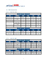
Страница 2: ...TION 3 2 2 SPECIFICATIONS 4 3 ELECTRICAL CHARACTERISTICS 4 3 1 INPUT VOLTAGE 4 3 2 RF CHARECTERISTICS 5 3 2 1 802 11B 11M 5 3 2 2 802 11G 54M 5 3 2 3 802 11N MCS7 HT20 6 3 2 4 802 11N_MCS7 HT40 6 4 PI...

Страница 3: ...parameters High data processing ability MCU frequency 580MHz 150M Mbps Support 802 11b g n mode 20 40 channel bandwidth Support 802 11v Support AP STA and AP STA mixed Fifth 10 100M adaptive com port...

Страница 4: ...2 HLK RM08S 2 Block diagram HLK RM08S Block Diagram EINT Ethernet UART GPIO PWM USB_HOST SPI SPIS I2C I2S JTAG SDXC MT7688KN 3 3V 40MHz SPI Flash 32MB IPEX Connector...

Страница 5: ...3 HLK RM08S 2 1 Typical application HLK RM08S typical peripheral interfaces diagram HLK RM08S...

Страница 6: ...b Flash 32Mb RF 1T1R 802 11n 2 4GHz USB2 0 1 UART 2 Temperature Environmental temperature 40 85 Humidity working 10 95 noncondensing Storage 5 95 noncondensing Size 17 4mm 25 8mm 2 8mm 3 Electrical ch...

Страница 7: ...802 11b Receiver Conductive Item Condition Min Typ Max Unit Frequency Range Channel 1 Channel 13 Min Input 11Mbps PER 8 91 5 89 5 87 5 dBm 3 2 2 802 11g 54M 802 11g Transmit Conductive Item Condition...

Страница 8: ...ndition Min Typ Max Unit Frequency Range Channel 1 Channel 13 Min Input MCS7 PER 10 76 5 74 5 72 5 dBm 3 2 4 802 11n_MCS7 HT40 802 11n_HT40 Transmit Conductive Item Condition Min Typ Max Unit Frequenc...

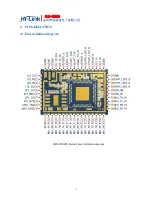
Страница 9: ...7 HLK RM08S 4 PINS DEFINTION 4 1 Pins definition diagram HLK RM08S Default pins definition diagram...

Страница 10: ...rial port TR 11 GPIO0 REF_CLKO PERST_N GPIO11 12 MDI_RP_P0 GPIO24 13 MDI_RN_P0 GPIO23 14 MDI_TP_P0 GPIO22 15 MDI_TN_P0 GPIO21 16 MDI_TP_P1 SPIS_CS PWM_CH0 GPIO14 17 MDI_TN_P1 SPIS_CLK PWM_CH1 GPIO15 1...

Страница 11: ...JTAG_TDO GPIO34 Com 0 status led 37 GND 38 GND 39 3 3V Suggested external power supply current 500mA 40 3 3V 41 WLED_N GPIO35 WiFi status LED 42 EPHY_LED1 JTAG_TDI GPIO33 Com 1status LED 43 EPHY_LED3...

Страница 12: ...space 1 4mm depth 1 8mm 2 The thickness of the module is 1 8mm 3 The noted numbers in the picture is the actual size of module do recommended pad extension around 1mm internal heat shrink 0 2mm pad i...

Страница 13: ...fixed device is defined as a device is physically secured at one location and is not able to be easily moved to another location Note 2 Any modifications made to the module will void the Grant of Cert...

Страница 14: ...Note 6 FCC ID label on the final system must be labeled with Contains FCC ID 2AD56HLK RM08S or Contains transmitter module FCC ID 2AD56HLK RM08S...

Отзывы: