


GD32F20x User Manual
270
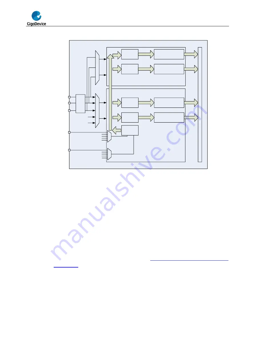
Figure 14-15. ADC sync block diagram
ADC_IN0
ADC_IN1
·
·
·
ADC_IN15
GPIO
V
SENSE
V
REF
EXTI_11
EXTI_15
A
P
B
B
U
S
ADC0
(master)
ADC1
(slave)
Regular data registers
(
16 bits
)
Inserted
channels
Injected data registers
(
16 bits x 4
)
Regular
channels
Regular data registers
(
16 bits
)
Inserted
channels
Injected data registers
(
16 bits x 4
)
Regular
channels
Regular
trigger mux
Inserted
trigger mux
Syncl mode
control
14.5.1.
Free mode
In this mode, the ADC synchronization is bypassed, and each ADC works freely.
14.5.2.
Regular parallel mode
This mode converts the regular channel simultaneously. The source of external trigger comes
from the regular group MUX of ADC0 (selected by the ETSRC[2:0] bits in the ADC_CTL1
register). A simultaneous trigger is provided to ADC1.
At the end of conversion event on ADC0 or ADC1 an EOC interrupt is generated (if enabled
on one of the two ADC interfaces) when the ADC0/ADC1 regular channels are all converted.
The behavior of regular parallel mode shows in the
Figure 14-16. Regular parallel mode on
A 32-bit DMA is used, which transfers ADC_RDATA 32-bit register (the ADC_RDATA 32-bit
register containing the ADC1 converted data in the upper half-word and the ADC0 converted
data in the lower half-word) to SRAM.
Note:
1. Do not convert the same channel on the two ADCs (no overlapping sampling times for the
two ADCs when converting the same channel).
2. In parallel mode, exactly the same sampling time should be configured for the two channels
Содержание GD32F20 Series
Страница 1: ...GigaDevice Semiconductor Inc GD32F20x ARM Cortex M3 32 bit MCU User Manual Revision 2 2 Oct 2019 ...
Страница 191: ...GD32F20x User Manual 191 Bits Fields Descriptions 31 0 TRNDATA 31 0 32 Bit Random data ...
Страница 290: ...GD32F20x User Manual 290 conversion is ongoing ...
Страница 325: ...GD32F20x User Manual 325 15 0 ALRM 15 0 RTC alarm value low ...
Страница 385: ...GD32F20x User Manual 385 ...
Страница 523: ...GD32F20x User Manual 523 clears AERR bit by writing 0 to it ...


