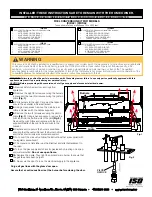
Schematic
BOM
R1
4M7
R2
1K
R3
680K
R4
680K
R5
470R
R6
100K
R7
100K
R8
470K
R9
10K
R10
47K
R11
47K
R12
47K
R13
47K
R14
47K
R15
680K
R16
680K
R17
15K
R18
1K
R19
33K
R20
470R
R21
2K2 (CLR)*
C1
47n
C2
1n5
C3
47n
C4
47n
C5
47p
C6
47n
C7
6n8
C8
2n2
C9
10n
C10
47n
C11
100p
C12
100n
C13
22u elec
C14
22u elec
C15
4u7 elec
C16
4u7 elec
Q1-3
2N3904
IC1
TL072
D1
1N4148
D2
1N4001
FUZZ
1KB
VOL
10KA
TONE
100KB
T1
1K Trim
SWITCH
3P4T Rotary
*If using a footswtich daughterboard you should solder R21 in the CLR position on
that instead of the main PCB.
Do not solder in Q2 until you read the notes on page 4 regarding the small hack
required to get the circuit working. Oops!
Alterations have been made to the output stage
of the op amp circuit to increase volume as the
original was a bit lacking. Thanks to Plesur and
his Feta Complis document for those details.