background image


10

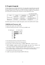
5. Program Upgrade 

The three programs are used for the SC-50/110. Two programs are used in the processor unit 
and one program is in the display unit. The program numbers are tabulated below. Note that 
the program number of SC-50 is the same as SC-110, but they are different. The program for 
SC-50 cannot be overwritten by the one for SC-110 in the field and vise versa.     
 

(As of February 2005)


Unit 

Board 

Program No. 

How to update 

MAIN board 

205-1341-01.02 

By using a PC 

Processor unit 

GPS receiver 

4850263003 

By replacing GPS core 

Display unit 

CPU board 

205-1342-01.01 

By using a PC 


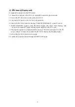
The following describes how to update the programs stored on the MAIN and CPU boards. 


1) MAIN board (Processor unit) 

To upgrade the program on the MAIN board; 


1. Connect the serial port of the PC to J15 (D-sub) on MAIN board 


PC (Serial port)      SC-50/110 (J15) 

#3                                #2 RXD 
#2                                 #3 TXD 
#6                                 #5 GND 
#4 
#6 
#7 
#8


2. Turn on the PC. Do not as yet turn on the SC-50/110.     

3. Click the SCUP.bat file in the SC-50/110 program file. 

4. Turn on the SC-50/110 after the message “TARGET POWER ON” on the PC screen. 

5. “NOW LOADING” appears on the SC-50/110 display unit, while “Now Erasing”, and 

“xxx percent completed” appear during program upgrade on the PC screen. 

6. The program upgrade is completed with the message “Finish Version up.ted” on the PC 

screen. (About 3 minutes 30 seconds) The SC-50/110 displays the Heading display. 

7. Turn off the SC-50/110 and turn it on again. 

8. Confirm the program number through the SOFT VER. menu.


Содержание Satellite Compass SC-50/110

Страница 1: ...SATELLITE COMPASS SC 50 110...

Страница 2: ...elephone 0798 65 2111 0798 65 2111 Fax Fax 0798 65 4200 0798 65 4200 FIRST EDITION FIRST EDITION NOV NOV 2005 2005 Printed in Japan Printed in Japan All rights reserved All rights reserved Pub No Pub...

Страница 3: ...ogram Upgrade 10 1 MAIN board 10 2 CPU board 11 6 Maintenance 12 6 1 Adjustment 12 6 2 Line voltage check 12 6 3 Jumper setting 12 6 4 LED 12 7 Location of Parts 13 Appendix 1 Protection of ICs in Dat...

Страница 4: ......

Страница 5: ...0 3 NAV 1 1 sec 4800 bps Output connector Terminal board Waterproof connector Processor unit W 300 B 200 H 60 W 335 B 265 H 103 Factory default setting Wall Bulkhead mount Floor mount Output of Headin...

Страница 6: ...lay Figure 2 shows MONITOR menu Fig 3 MONITOR menu SC OUT Output of the satellite compass degree GPS Values calculated by using GPS signal degree ANG V Angular velocities of rate sensors degree sec R...

Страница 7: ...NST SDEV S SDEV C and CHK NEW SV Fig 4 COMPASS display 3 R MONITOR display Rate sensor Monitor display shows rate sensor errors as below WA SHIFT Shows the difference between GPS and rate sensor DIFF...

Страница 8: ...t factory It is not necessary to change this value when the rate sensor is replaced with new one However the value on top of the original sensor is written on top of the replacement sensor for future...

Страница 9: ...xample below an alarm is generated when the difference is 1 00 or more Fig 8 Rate error display When the rate sensor error appears after the installation first check that the rate sensor is mounted an...

Страница 10: ...rts If necessary enter the Offset value digital value 9 ANT MONI display Figure 12 shows an example of Antenna Monitor display 1 01 BOW 0 91 01 02 03 04 05 06 07 08 09 10 11 12 11 1 2 3 4 5 6 7 8 9 10...

Страница 11: ...th reflection It is around 1 0 normally If it is 1 5 or above the antenna must be relocated because the system is affected by the multipath reflection The left figure is the index for the baseline 2 a...

Страница 12: ...defective The number of the satellite being used for heading calculation is displayed at the right hand side below CAL and the number of the satellite being tracked below ALL The system requires 4 or...

Страница 13: ...about 24 hours If the data is transferred to the flash memory they are not erased during the replacement Parts Name Type Code No Lithium Battery CR2450 F2ST2L 000 144 941 To transfer the memory 1 Choo...

Страница 14: ...grams stored on the MAIN and CPU boards 1 MAIN board Processor unit To upgrade the program on the MAIN board 1 Connect the serial port of the PC to J15 D sub on MAIN board PC Serial port SC 50 110 J15...

Страница 15: ...e SC 50 110 after the message TARGET POWER ON on the PC screen 5 NOW LOADING appears on the SC 50 110 display unit while Now Erasing and xxx percent completed appear during program upgrade on the PC s...

Страница 16: ...est Point GND Rating Adjuster 1 of J20 2 of J20 5 0 V Vcc c VR96 6 2 Line voltage check Line voltages are checked at J3 on the MAIN board Line voltage Test Points on MAIN board Rating 3 3 V 4 and 5 of...

Страница 17: ...ault Pitch GPS Receivers 1 2 3 from Top Rate Sensor Default Roll Rate Sensor Default Yaw Main Board 20P8178 PWR Board 20P8181 Fig 17 Processor Unit with cover removed Fig 18 PWR Board 20P8181 TP2 TP1...

Страница 18: ...178 BT1 CR2450 F2ST2L Roll above Pitch Log Alarm Beacon Ext Data out 1 to 5 Data In from right IEC or AD 10 Heading data J15 for system update J20 J19 J18 TP1 R96 No short bar for R D Data out 6 AD 10...

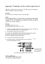
Страница 19: ...tallation Carry out 1 to 4 When the symptom occurs Carry out 1 to 5 1 Solder a grounding cable to the cable shield and ground it through the screw fixing the MAIN board See the attached sheet 2 Ground...

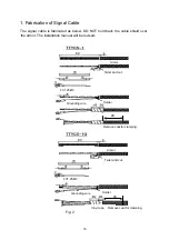
Страница 20: ...NOT hold back the cable shield over the armor The installation manual will be revised 80 80 40 70 70 40 Twist and cut Armor FV1 25 M3 Solder Grounding wire Remove coat for clamping FV1 25 M3 Armor Gr...

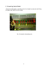
Страница 21: ...17 2 Grounding Cable Shield Ground the cable shield or grounding wire to the chassis by using the screw fixing the MAIN board 20P8178 to the chassis Fig 3 Connection of grounding wire...

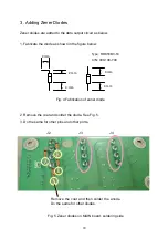
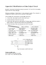
Страница 22: ...gure below Type RD9 1EB3 T4 C N 000 138 700 Fig 4 Fabrication of zener diode 2 Remove the coat and solder the diode See Fig 5 3 Do the same for other pins and other ports 2 mm 4 mm 4 mm 4 mm 4 mm Remo...

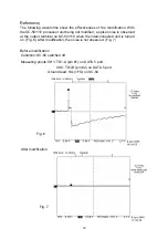
Страница 23: ...noise is observed at the output terminal on SC 50 110 when the interconnected unit is turned on Fig 6 After modification the noise is not observed Fig 7 Before modification Condition SC 50 switched o...

Страница 24: ...e shield to FG when data is IEC61162 1 AD 10 photo coupler or SG when data is IEC61162 2 RS422 485 4 Ground the frame of the unit connected to SC 50 110 securely Before modification After modification...

Страница 25: ...0 147 431 231 305 026 FUR 000 147 431 231 CONNECTOR 231 306 026 FUR 000 147 430 231 CONNECTOR 231 302 026 FUR 000 148 883 CASE 20 024 2002 4 100 310 674 CONNECTOR PH 7P M J7P L 260 000 148 552 MINI CL...

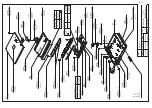
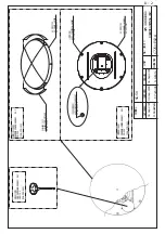
Страница 26: ...NA UNIT C 7251 E02 A F U N O RADOME COVER ASSEM B LY SC 303 004 378 120 RADOME LOWER ASSEM B LY SC 303 004 378 140 GPS GPS ANTENNA ASSEM B LY GSC 00 1 004 382 480 SC SC DOME UPPER 20 020 3111 1 FURUNO...

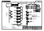
Страница 27: ...DATA1 C TD1 B DATA5 H TD9 A DATA5 C TD9 B SHIFT5 H TD10 A SHIFT5 C TD10 B TTYCS 1 TTYCS 1 PITCH SG J12 PITCH ROLL J11 SG ROLL 2 1 2 1 J9 DATA IN AD 10 only RADAR CURRENT INDICATOR ETC J10 LOG ALARM F...

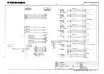
Страница 28: ...S 2...

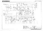
Страница 29: ...S 3...

Страница 30: ...S 4...

Отзывы: