


34 Canyon View Drive Orinda, CA., 94563 p:925.253.2969 f:925.253.4894
LOW LEVEL SOFTWARE INTERFACE (MOST
USERS NEED NOT READ)
The SYNTH300 board is easy to communicate with. In most cases, this section may be skipped, as
the driver supplied with the board will automatically handle all communication with the board registers.
The best way to develop your own custom software is simply to modify the included example program,
example.cpp, using the functions from SynthAPI.cpp and then rebuild the application. However, the
following section gives an overview of how the driver calls control the board.
The software interface consists of a PCI type-00 Configuration Header and a Control Register..
Accesses to Control and Auxiliary registers must be made as 32-bit transfers.
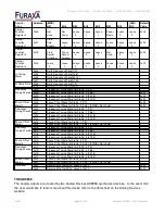
PCI CONFIGURATION HEADER
SYNTH300 series boards support a PCI Configuration Header, whose map is shown below..
Double Word
Address
byte 3
byte 2
byte 1
byte 0
00 H
Device ID
Vendor ID
04 H
Status
Command
08 H
Class Code
Revision ID
0C H
Header Type
Latency Timer
10 H
Base Address for memory-mapped control register
14 H
18 H
1C H
20 H
24 H
28 H
2C H
30 H
34 H
38 H
3C H
Max Lat (=01 H)
Min Gnt (=01 H)
Interrupt Pin
Interrupt Line
The board control register is mapped at configuration space address 80H, as well as in memory space
at Base A 1FFFFFC. The Auxiliary register is mapped at configuration space address 8CH,
and in memory space at Base A 1FFFFF4 Accessing either place will read or write these
registers. .
Double Word
Address
byte 3
byte 2
byte 1
byte 0
80 H
SYNTH300 Control Register |
84 H
Auxiliary Register
r1v06
Page 26 of 31
Copyright © 2008 – 2010 Furaxa Inc.