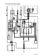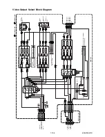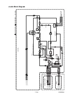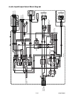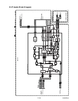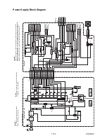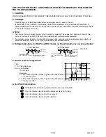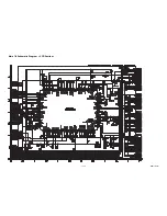
background image

1-11-17

E9G01TR

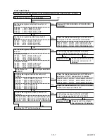
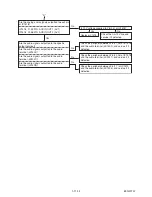
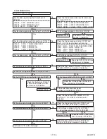
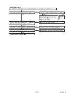
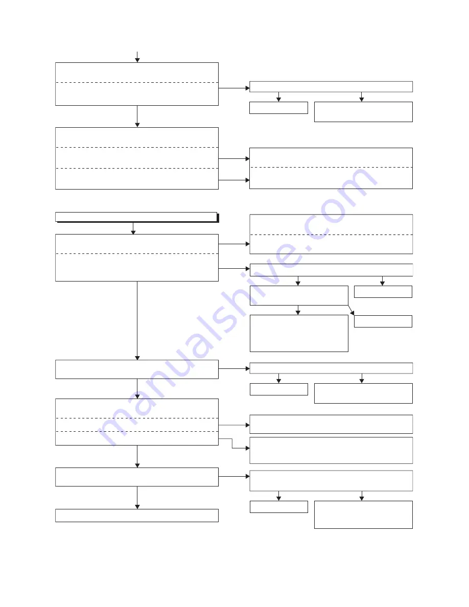
FLOW CHART NO.11                           

Hi-Fi E-E audio does not operate normally. 

No

Check the periphery of JK1502 from Pin(29) of 
IC1518 and service it if defective.

Are the video signals outputted to the specific 
output terminal?

Are the composite video signals outputted to the 
VIDEO-OUT terminal (JK1502)?

Are the composite video signals outputted to the 
VIDEO-OUT terminal (JK2001)?

Yes

IC1518   29PIN   VIDEO-OUT 1 (AV1)
IC1518   30PIN   VIDEO-OUT 2 (AV2)

Are the video signals outputted to each pin 
of IC1518?

No

No

Check the periphery of JK2001 from Pin(30) of 
IC1518 and service it if defective.

No

Check the AL+12V(1) line 
and service it if defective.

Replace IC1518.

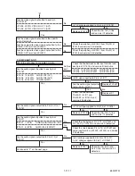
Yes

No

Is 12V voltage supplied to Pin(2,4) of IC1518?

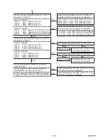
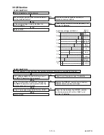
"E"

Is SIF signal inputted to Pin(2) of IC1?

Are the audio signal outputted 
to Pin(30,31) of IC1?

Replace TU1501.

Replace IC1.

Yes

Check the line between 
Pin(30,31) of IC1 and 
Pin(20,24) of IC1518, and 
service it if defective.

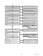
Yes

No

No

Check the AL+12V(1) line 
and service it if defective.

Replace IC1518.

Yes

No

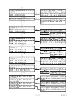
Are the audio signals inputted to each pin of 
IC1518?

Check the line between audio input terminal and 
each pin of IC1518, and service it if defective.

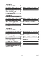
Check the line between Pin (1,12) of IC1501 and 
Pin (23,27) of IC1518, and service it if defective. 

Are the audio signals outputted to Pin(23,27) of 
IC1518?

Yes

Yes

Yes

Yes

No (Rear 
input)

No (Tuner)

No

No

Check the  line between Pin (5,14) of IC1501 and 
audio input terminal (JK1202, JK1203), and service 
it if defective. 

No

IC1518

AUDIO-IN1 (AV1)

10,16PIN

IC1518

AUDIO-IN2 (AV2)

8,14PIN

IC1518

TUNER-AUDIO

20,24PIN

Are the audio signals inputted to each pin of 
IC1501?

IC1501

TUNER-AUDIO/AUDIO-IN1,2

1,12PIN

IC1501

AUDIO-IN-F (FRONT)

5,14PIN

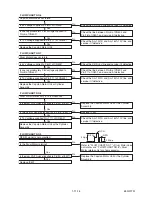
IC1518

JK1502

10,16PIN

IC1518

JK2001

8,14PIN

AUDIO-IN1 (AV1)
AUDIO-IN2 (AV2)

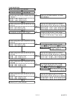
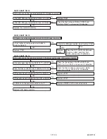
Is 12V voltage supplied to Pin(2,4) of  IC1518? 

Check the AL+5V(1) and 
AL-5V line, and service it if 
defective.

Replace IC1501.

Yes

No

Are the audio signals outputted to Pin(3,13) of 
IC1501?

Is 5V voltage supplied to Pin(16) of IC1501? 
Is -5V voltage supplied to Pin(7) of IC1501? 

Continued to "F" on the next page.

Содержание DRVR-B778S

Страница 1: ...R B778S Main Section I Specifications I Preparation for Servicing I Adjustment Procedures I Schematic Diagrams I CBA s I Exploded views I Parts List When servicing the deck mechanism refer to MK14 Dec...

Страница 2: ...icator Symbols 1 10 1 Troubleshooting 1 11 1 Block Diagrams 1 12 1 Schematic Diagrams CBA s and Test Points 1 13 1 Waveforms 1 14 1 Wiring Diagram VCR Section 1 15 1 Wiring Diagram DVD Section 1 15 2...

Страница 3: ...de W O Burst 1 4 Video Color S N AM R P dB 37 41 SP Mode 1 5 Video Color S N PM R P dB 30 36 SP Mode 1 6 Resolution PB Line 230 245 SP Mode 2 Servo 2 1 Jitter Low sec 0 07 0 12 SP Mode 2 2 Wow Flutter...

Страница 4: ...load Vp p 1 0 C Chrominance 75 load Vp p 0 3 2 AUDIO 2 1 Output Level Vrms 2 0 2 2 Frequency Response DVD VIDEO LPCM fs 96 kHz Hz 20 44 k fs 48 kHz Hz 20 20 k Audio CD fs 44 1 kHz Hz 20 20 k 2 3 Signa...

Страница 5: ...y from the pickup lens when the diode is turned on Do not look directly at the laser beam CAUTION Use of controls and adjustments or doing procedures other than those specified herein may result in ha...

Страница 6: ...cal for safety Replace only with part number specified B In addition to safety other parts and assemblies are specified for conformance with regulations applying to spurious radiation These must also...

Страница 7: ...2 Leakage Current Test Confirm the specified or lower leakage current between B earth ground power cord plug prongs and externally exposed accessible parts RF termi nals antenna terminals video and a...

Страница 8: ...achine then apply hot air to the Flat Pack IC about 5 to 6 seconds Fig S 1 1 2 Remove the flat pack IC with tweezers while applying the hot air 3 Bottom of the flat pack IC is fixed with glue to the C...

Страница 9: ...by one using a sharp pin or wire to which solder will not adhere iron wire When heating the pins use a fine tip soldering iron or a hot air desoldering machine Fig S 1 4 3 Bottom of the flat pack IC i...

Страница 10: ...s Fig S 1 6 Note When using a soldering iron care must be taken to ensure that the flat pack IC is not being held by glue When the flat pack IC is removed from the CBA handle it gently because it may...

Страница 11: ...ed to remove any static electricity that may be charged on the body 2 Ground for Workbench Be sure to place a conductive sheet or copper plate with proper grounding 1 M on the workbench or other surfa...

Страница 12: ...o the Deck Mechanism Assembly and press the PLAY VCR button The tape will be loaded into the Deck Mechanism Assembly Make sure the power is on connect TP501 S INH to GND This will stop the function of...

Страница 13: ...4 5 Front Jack CBA D3 Jack Earth Plate 6 DVD Mechanism DVD Main CBA Assembly D4 4 S 5 CN101 CN701 4 7 Dust Cover D4 8 Rear Panel Unit D5 3 S 6A 2 S 6B 3 S 7 S 8 CN1503 9 Fan Holder D6 3 S 9 10 Motor...

Страница 14: ...D9 Then install the Deck Assembly while aligning the hole of Cam Gear with the pin of LD SW the shaft of Cam Gear with the hole of LD SW as shown in Fig D9 4 The DVD Mechanism DVD Main CBA Assem bly i...

Страница 15: ...7 S 7 S 7 CN1503 S 8 8 Rear Panel Unit Fig D6 S 9 11 Rear Panel 10 Motor DC Fan 9 Fan Holder CN1504 Fig D7 S 11 S 10 12 Power Supply CBA 13 PCB Holder Fig D8 S 12 S 15 S 16 S 14 S 14 S 13C PCB Washer...

Страница 16: ...E Head BOTTOM VIEW Lead connections of Deck Assembly and Main CBA Desolder From Capstan Motor Assembly Printing side Desolder From Cylinder Assembly From ACE Head Assembly Lead with blue stripe Lead w...

Страница 17: ...1 6 5 E9G01DC Fig D10 20 Deck Pedestal 21 Front Bracket R S 19 S 19 S 19 S 19 S 20...

Страница 18: ...the Front Bracket 4 Remove the DVD Mechanism DVD Main CBA Assembly 5 Unhook two places and detach the Dust Cover 6 Rotate the gear in the direction of the arrow manually as shown below until the tray...

Страница 19: ...0 001 50V Div F Range DC AC 20MHz 2 Alignment Tape FL6A Head Switching Position Adjustment Purpose To determine the Head Switching position during playback Symptom of Misadjustment May cause Head Swi...

Страница 20: ...tializing is completed the DVD recorder exits the Version display mode and turns off the power automatically To move into the Normal mode from the Version display mode press RETURN button on the remot...

Страница 21: ...scribed as follows 5 After updating is finished the tray opens automatically At this time no button is available 6 Pull out the AC code once then insert it again Fig a Version Up Mode Screen Firmware...

Страница 22: ...E When reel or capstan mechanism is not functioning correctly A R is displayed on a TV screen Refer to Fig 1 When tape loading mechanism is not func tioning correctly A T is displayed on a TV screen R...

Страница 23: ...able 14 Cannot write the data after recovering SMALL VMGI 15 Cannot write the data after DVD R Reverse Track 16 An error occurs in Finalize Close 17 An error occurs in Rec Stop Close 18 An error occur...

Страница 24: ...e unnecessary titles 34 There is not space to record field of control information 10 You cannot record on the disc as Power Calibration Area is full Insert a new disc 35 PCA is Full in REC start 4 Thi...

Страница 25: ...ing diode or circuit is shorted in each rectifying circuit of secondary side and service it if defective FLOW CHART NO 3 When the output voltage fluctuates No Yes Does the secondary side photo coupler...

Страница 26: ...inputted to the base of Q1518 Check D015 D016 D1032 L013 C018 and their periphery and service it if defective Check R1523 and their periphery and service it if defective FLOW CHART NO 7 P ON 9V is no...

Страница 27: ...ly 500kHz oscillation to Pin 5 of IC612 Are the filament voltage applied between Pin 1 and Pin 24 of the fluorescent display tube Also negative voltage applied between these pins and GND Replace the f...

Страница 28: ...he RM1501 remote control receiver and Pin 14 of IC501 and service it if defective Is the L pulse sent out from Pin 1 terminal of the RM1501 remote control receiver when the remote control unit is acti...

Страница 29: ...o B on the FLOW CHART NO 6 Picture does not appear normally In the RGB Component video output JK1501 JK1502 Yes Yes No Is 12V voltage supplied to Pin 2 4 of IC1518 No No IC1518 1PIN VIDEO IN1 AV1 IC15...

Страница 30: ...VIDEO C OUT Check the line between each pin of IC1515 and each pin of CN1502 and service it if defective IC1515 3PIN CN1502 1PIN VIDEO Y I OUT IC1515 1PIN CN1502 9PIN VIDEO C OUT Are the video signal...

Страница 31: ...to JK1501 IC1510 13PIN VIDEO Y I P OUT IC1510 3PIN VIDEO Pr Cr OUT IC1510 1PIN VIDEO Pb Cb OUT IC1509 2PIN VIDEO Y I P OUT IC1509 12PIN VIDEO Pr Cr OUT IC1509 5PIN VIDEO Pb Cb OUT IC1509 1PIN VIDEO G...

Страница 32: ...3PIN VIDEO Pr Cr OUT IC1516 6PIN IC1510 1PIN VIDEO Pb Cb OUT Are the video signals inputted to each pin of IC1516 and each pin of IC1514 Output to JK1501 IC1516 3PIN VIDEO Y I P OUT IC1516 8PIN VIDEO...

Страница 33: ...Yes Yes Yes Yes No Rear input No Tuner Replace IC1506 No No No Check the line between Pin 5 14 of IC1501 and audio input terminal JK1202 JK1203 and service it if defective No IC1518 AUDIO IN1 AV1 10...

Страница 34: ...1508 and each pin of IC1518 and service it if defective IC1508 15PIN IC1518 6PIN AUDIO L OUT IC1508 14PIN IC1518 12PIN AUDIO R OUT No IC1518 21 25PIN AUDIO OUT 1 AV1 IC1518 22 26PIN AUDIO OUT 2 AV2 Ar...

Страница 35: ...13PIN AUDIO R OUT Are the analog audio signals inputted to each pin of IC1508 Yes No Yes No No Do Pin 26 29 of IC501 become H level If Pin 26 of IC501 become L level replace DVD MECHANISM DVD MAIN CBA...

Страница 36: ...io signals outputted to the audio terminal JK1505 Yes IC1518 21 25PIN AUDIO OUT 1 AV1 IC1518 22 26PIN AUDIO OUT 2 AV2 Are the analog audio signals outputted to each pin of IC1518 No No Check the perip...

Страница 37: ...EW PLAY CH DOWN STOP EJECT Terminal voltage of IC501 7 KEY 1 IC501 7 V Replace the RM1501 remote control receiver Replace remote control unit if need Check the line between the RM1501 remote control r...

Страница 38: ...t if defective While the Takeup Reel is rotating is the reel pulse signal inputted to Pin 80 of IC501 While the reel pulse signal is inputting is L pulse outputted to Pin 81 of IC501 Is the specified...

Страница 39: ...e and service it if defective Check the P ON 5V line and service it if defective Check the line between Pin 8 of CN502 and Pin 77 of IC501 and service it if defective Replace IC501 No No No No No No N...

Страница 40: ...efective Yes Check the AL 5V 1 and AL 5V line and service it if defective Replace IC1508 Yes No Is 5V voltage supplied to Pin 16 of IC1508 Is 5V voltage supplied to Pin 7 of IC1508 Yes Yes Continued t...

Страница 41: ...o No Check the AL 12V 1 line and service it if defective Replace IC1518 Yes No Are the audio signals inputted to each pin of IC1518 Check the line between audio input terminal and each pin of IC1518 a...

Страница 42: ...16 32 35 36 46 55 of IC451 or the 9V voltage supplied to Pin 69 of IC451 Is the serial data and the clock signal supplied to Pin 37 38 of IC451 Is the audio signal outputted to Pin 74 76 of IC451 Is t...

Страница 43: ...utted to Pin 100 of IC301 Yes Yes Replace ACE head assembly Yes Yes No No No No Check the Hi Fi H SW line between Pin 39 of IC451 and Pin 19 of IC501 and service it if defective Check the line between...

Страница 44: ...f ACE head assembly Is the audio signal supplied to Pin 5 of IC301 Replace IC301 Is the audio signal outputted to Pin 11 of IC301 Check the line between Pin 11 of IC301 and Pin 80 of IC451 and service...

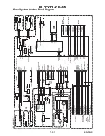
Страница 45: ...D V SYNC D REC H RF SW H A SW C ROTA IIC BUS SDA H A COMP V ENV 24 DAVN L DAVN L DVD AUDIO MUTE DVD SCART AUDIO MUTE 30 C SYNC C SYNC IIC BUS SCL LD SW 9 AL 5V SW507 LD SW AL 5V D555 S LED TP501 RM150...

Страница 46: ...SDRAM CN201 DVD MECHANISM TILT TRACKING FOCUS PICK UP SLED MOTOR M REC VIDEO SIGNAL PB VIDEO SIGNAL REC AUDIO SIGNAL PB AUDIO SIGNAL D A LPC CN1001 CN701 SPINDLE MOTOR M CN1002 CN301 3 3V IC701 VIDEO...

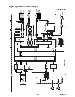
Страница 47: ...DEO L 1 HEAD VIDEO L 2 HEAD VIDEO R 2 HEAD VIDEO L 2 VIDEO COM VIDEO R 2 4 5 6 IC301 VIDEO SIGNAL PROCESS HEAD AMP IC501 OSD VCR VIDEO VCR VIDEO DUB VCR DVD DUBBING DVD VIDEO DUB PB EE VIDEO REC VIDEO...

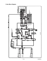
Страница 48: ...Y IN 1 1 FRONT C IN 4 4 FRONT VIDEO IN CN1201 Q1520 Q1521 BUFFER VIDEO SW1 IC1518 VIDEO INPUT SELECT IC1508 SW 29 33 32 28 1 3 5 30 31 6dB AMP CONTROL LOGIC SW CTL 6dB AMP DRIVER BUFFER DRIVER JK1502...

Страница 49: ...AMP 2dB AMP LPF DRIVER 6 8dB AMP 6dB DRIVER 4dB AMP 2dB AMP LPF DRIVER 3 1 7 13 4dB AMP 2dB AMP LPF DRIVER 11 4dB AMP 2dB AMP LPF DRIVER 6 10 4dB AMP 2dB AMP LPF DRIVER 8 1 15 15 1 2 4 9 10 11 3 5 IC...

Страница 50: ...MUTE 11 6 PB ON SP LP ON P TUNER IN2 IN1 R ALC DET ALC IC301 AUDIO SIGNAL PROCESS HEAD AMP 15 13 17 4 AUDIO PB REC CN504 3 A COM 1 AE H 2 AE H FE H AUDIO HEAD AUDIO ERASE HEAD ACE HEAD ASSEMBLY FE HE...

Страница 51: ...MP IC1513 SW IC1508 OP AMP OP AMP 2 6 1 7 TO SERVO SYSTEM CONTROL BLOCK DIAGRAM TO Hi Fi AUDIO BLOCK DIAGRAM WF8 Q1537 Q1507 MUTE ON Q1538 MUTE ON Q2002 MUTE ON Q2003 MUTE ON IF SIGNAL PROCESS CN1506...

Страница 52: ...R DVD VCR DUBBING VCR AUDIO R DVD AUDIO L VCR AUDIO L LIM 80 N A PB Hi Fi H SW AUDIO MUTE 2 A MODE TO AUDIO BLOCK DIAGRAM TO AUDIO INPUT OUTPUT SELECT BLOCK DIAGRAM TO AUDIO INPUT OUTPUT SELECT BLOCK...

Страница 53: ...25 25 AL 3V 26 26 AL 3V 31 31 AL 4V 32 32 AL 4V 34 34 F1 33 33 F2 2 2 AL 12V 3 3 AL 12V 6 6 FAN AL 12V 7 7 FAN AL 12V 8 8 FAN AL 12V TO SERVO SYSTEM CONTROL BLOCK DIAGRAM TO SERVO SYSTEM CONTROL BLOCK...

Страница 54: ...stitute replacement parts that do not have the same safety characteristics as specified in the parts list may create shock fire or other hazards Notes 1 Do not use the part number shown on these drawi...

Страница 55: ...acement parts which are listed with their part numbers in the parts list section of the service manual 4 Voltage indications for PLAY and REC modes on the schematics are as shown below 5 How to read c...

Страница 56: ...1 13 3 E9G10SCM1 Main 1 9 Schematic Diagram VCR Section...

Страница 57: ...g c d e f g h h i a b a b a b a b a b FL601 MATRIX CHART REPEAT PM REC VCD VCR DVD R XP SP LP EP SLP P SCAN SEP W CD T C 5G 4G 3G 2G 1G 7G 6G a d g h h g c b e f REPEAT PM REC VCD VCR DVD R XP SP LP...

Страница 58: ...1 13 5 E9G10SCM3 Main 3 9 Schematic Diagram VCR Section...

Страница 59: ...1 13 6 E9G10SCM4 Main 4 9 Schematic Diagram VCR Section...

Страница 60: ...1 13 7 E9G10SCM5 Main 5 9 Schematic Diagram VCR Section...

Страница 61: ...1 13 8 E9G10SCM6 Main 6 9 Front Jack Schematic Diagram VCR Section...

Страница 62: ...1 13 9 E9G10SCM7 Main 7 9 Schematic Diagram VCR Section...

Страница 63: ...1 13 10 E9G10SCM8 Main 8 9 Schematic Diagram VCR Section...

Страница 64: ...1 13 11 E9G10SCM9 Main 9 9 Schematic Diagram VCR Section...

Страница 65: ...k to see that all components in the power supply circuit are not defective before you connect the AC plug to the AC power supply Otherwise it may cause some components in the power supply circuit to f...

Страница 66: ...1 13 13 E9G10SCRJ Rear Jack Schematic Diagram VCR Section...

Страница 67: ...1 13 14 E9G10SCAFV AFV Schematic Diagram VCR Section...

Страница 68: ...n 1 5 Schematic Diagram DVD Section The order of pins shown in this diagram is different from that of actual IC101 IC101 is divided into five and shown as IC101 1 5 IC101 5 5 in this DVD Main Schemati...

Страница 69: ...n 2 5 Schematic Diagram DVD Section The order of pins shown in this diagram is different from that of actual IC101 IC101 is divided into five and shown as IC101 1 5 IC101 5 5 in this DVD Main Schemati...

Страница 70: ...n 3 5 Schematic Diagram DVD Section The order of pins shown in this diagram is different from that of actual IC101 IC101 is divided into five and shown as IC101 1 5 IC101 5 5 in this DVD Main Schemati...

Страница 71: ...n 4 5 Schematic Diagram DVD Section The order of pins shown in this diagram is different from that of actual IC101 IC101 is divided into five and shown as IC101 1 5 IC101 5 5 in this DVD Main Schemati...

Страница 72: ...n 5 5 Schematic Diagram DVD Section The order of pins shown in this diagram is different from that of actual IC101 IC101 is divided into five and shown as IC101 1 5 IC101 5 5 in this DVD Main Schemati...

Страница 73: ...1 13 20 SW POINT VR501 TP301 WF2 C PB CTL TP503 TP504 RF SW JK1 V OUT J236 WF3 S INH TP501 WF1 BHF300F01012B BHF300F01012A Main CBA Top View Sensor CBA Top View BE9G00F01012A...

Страница 74: ...1 13 21 PIN 5 OF CN1502 WF5 PIN 3 OF CN1502 WF6 PIN 7 OF CN1502 WF8 PIN 17 OF CN1502 WF7 PIN 9 OF CN1502 WF4 WF10 PIN 3 OF CN1501 WF9 PIN 6 OF IC1515 BE9G00F01012A Main CBA Bottom View...

Страница 75: ...1 13 22 BE9G00F01012C BE9G00F01012B BE9G00F01012D Front Jack CBA Top View Front Jack CBA Bottom View Power SW CBA Top View Power SW CBA Bottom View Function CBA Top View Function CBA Bottom View...

Страница 76: ...red CAUTION Fixed voltage or Auto voltage selectable power supply circuit is used in this unit If Main Fuse F1001 is blown check to see that all components in the power supply circuit are not defectiv...

Страница 77: ...ired CAUTION Fixed voltage or Auto voltage selectable power supply circuit is used in this unit If Main Fuse F1001 is blown check to see that all components in the power supply circuit are not defecti...

Страница 78: ...1 13 25 REAR JACK CBA Top View REAR JACK CBA Bottom View BE9B00F01022B AFV CBA Top View AFV CBA Bottom View BE6800F01091...

Страница 79: ...SPDIF 1V 0 1 s WF10 Pin 3 of CN1501 WF6 Pin 7 of CN1502 VIDEO Y 0 2V 20 s WF7 Pin 9 of CN1502 VIDEO C 0 2V 20 s WF9 Pin 6 of IC1515 VIDEO CVBS 0 5V 20 s WF2 WF3 UPPER WF1 WF1 LOWER J236 TP504 UPPER LO...

Страница 80: ...O L 5 TU AUDIO R 4 GND 3 2 SIF NU 1 9 8 7 6 5 4 3 2 1 FAN 12V 1 LOADING MOTOR CAPSTAN MOTOR M DRUM MOTOR PG SENSOR M CAPSTAN MOTOR MOTOR DRIVE CIRCUIT M CN1502 CN1501 1 2 3 4 5 6 7 8 9 10 11 12 13 14...

Страница 81: ...GND 5 GND 4 DVD P ON 3 3V 17 DVD P ON 3 3V 16 DVD P ON 3 3V 15 GND 28 GND 29 GND 30 PICKUP CN201 CN1001 10 9 HW 9 10 HW 1 FCS 4 TRK 3 TRK 2 FCS 6 TILT 5 TILT 7 LDD IIN4 9 LDD IIN2 10 LDD IINR 11 NU 8...

Страница 82: ...Select Signal 3 25 OUT REG CONT2 Power Regulator Control Signal 26 OUT DVD AUDIO MUTE DVD Audio Mute Control Signal 27 OUT RGB THROUGH SCART 2 RGB Through Control Signal 28 OUT AUDIO MUTE 2 Audio Mute...

Страница 83: ...m Motor Control Signal 78 OUT C F R Capstan Motor FWD REV Control Signal FWD L REV H 79 IN S REEL Supply Reel Rotation Signal 80 IN T REEL Take Up Reel Rotation Signal 81 OUT LM FWD REV Loading Motor...

Страница 84: ...DRV STB DRV Serial Interface Strobe 10 NU Not Used 11 NU Not Used 12 VSS Ground 13 VDD 5V Power Supply 14 NU Not Used 15 NU Not Used 16 NU Not Used 17 NU Not Used 18 NU Not Used 19 NU Not Used 20 OUT...

Страница 85: ...NSR CD4053BNSR MID 32A22F PT204 6B 12 FMG4A T148 RN1511 TE85R F 2SC2412K T146Z 2SC3928A T112 1Z KRC103S RTK P KTC3875S GR Y RTK P KTC3879 Y RTK P LA72648M MPB E MM1636XWRE 4052L S16 R 4053L S16 R MM16...

Страница 86: ...3 C 2L022 2L021 2L054 2L052 JW001 2L017 2L017 2L017 2L017 2L017 2L017 2B1 A1X JW002 JW103 F1001 RM1501 2B16 2B17 2B87 2B46 Main CBA Function CBA Front Jack CBA Rear Jack CBA Power Supply CBA Power SW...

Страница 87: ...1 18 2 E9G01PEX Packing X4 S2 S2 S3 S2 A14 S1 S5 S5 S2 X9 X3 S9 X2 X1 X31 X43 X22 X20 S10...

Страница 88: ...0 2L017 SCREW S TIGHT M3X8 BIND HEAD GBJS3080 2L021 SCREW P TIGHT M3X8 BIND HEAD GBCP3080 2L022 SCREW S TIGHT M3X6 BIND HEAD GBJS3060 2L030 SCREW P TIGHT M3X8 BIND HEAD GBJP3080 2L033 SCREW S TIGHT M3...

Страница 89: ...ECTROLYTIC 100 F 16V M CA1C101ENE12 C331 ELECTROLYTIC CAP 220 F 6 3V M or CE0KMASDL221 CAP ELECTROLYTIC 220 F 6 3V M CA0K221ENE12 C333 CHIP CERAMIC CAP 1608 F Z 0 1 F 50V CHD1JZ30F104 C334 ELECTROLYTI...

Страница 90: ...EZTFZ223 C518 ELECTROLYTIC CAP 22 F 6 3V M H7 or CE0KMAVSL220 CAP ELECTROLYTIC 22 F 6 3V M H7 CA0K220ENE10 Ref No Description Part No C519 CHIP CERAMIC CAP CH J 560pF 50V CHD1JJ3CH561 C520 CHIP CERAMI...

Страница 91: ...CTROLYTIC 4 7 F 25V M H7 CA1E4R7ENE10 C1572 ELECTROLYTIC CAP 10 F 16V M or CE1CMASDL100 Ref No Description Part No CAP ELECTROLYTIC 10 F 16V M CA1C100ENE12 C1573 ELECTROLYTIC CAP 10 F 16V M or CE1CMAS...

Страница 92: ...ECTROLYTIC CAP 4 7 F 25V M or CE1EMASDL4R7 CAP ELECTROLYTIC 4 7 F 25V M CA1E4R7ENE12 C1685 ELECTROLYTIC CAP 4 7 F 25V M or CE1EMASDL4R7 CAP ELECTROLYTIC 4 7 F 25V M CA1E4R7ENE12 C1686 ELECTROLYTIC CAP...

Страница 93: ...DZ11BS D1540 ZENER DIODE MTZJT 7711A or QDTA00MTZJ11 DIODE ZENER 11BSA T26 or NDTA011BST26 ZENER DIODE DZ 11BSAT265 NDTA00DZ11BS D1542 ZENER DIODE MTZJT 7711A or QDTA00MTZJ11 Ref No Description Part N...

Страница 94: ...SYKTC3199P TRANSISTOR KTC3199 GR AT P or NQS4KTC3199P TRANSISTOR 2SC1815 Y TE2 F T or QQSY2SC1815F Ref No Description Part No TRANSISTOR 2SC1815 GR TE2 F T QQS12SC1815F Q1515 TRANSISTOR KTC3199 Y AT P...

Страница 95: ...02 R411 CHIP RES 1 10W J 27k or RRXAJR5Z0273 RES CHIP 1608 1 10W J 27k RRXA273YF002 Ref No Description Part No R412 CHIP RES 1 10W J 120 or RRXAJR5Z0121 RES CHIP 1608 1 10W J 120 RRXA121YF002 R413 CHI...

Страница 96: ...S CHIP 1608 1 10W J 820 RRXA821YF002 R588 CHIP RES 1 10W J 470 or RRXAJR5Z0471 Ref No Description Part No RES CHIP 1608 1 10W J 470 RRXA471YF002 R595 CARBON RES 1 4W J 10k RCX4JATZ0103 R596 CARBON RES...

Страница 97: ...S 1 4W J 27 RCX4JATZ0270 R1555 CHIP RES 1 10W J 33k or RRXAJR5Z0333 Ref No Description Part No RES CHIP 1608 1 10W J 33k RRXA333YF002 R1556 CHIP RES 1 10W F 15k or RRXAFR5H1502 CHIP RES 1 10W F 15k or...

Страница 98: ...r RRXAFR5Z8200 RES CHIP 1608 1 10W F 820 RTW8200YF002 R1642 CHIP RES 1 10W J 10k or RRXAJR5Z0103 Ref No Description Part No RES CHIP 1608 1 10W J 10k RRXA103YF002 R1643 CARBON RES 1 6W J 15k or RCX6JA...

Страница 99: ...ES CHIP 1608 1 10W J 33k RRXA333YF002 SWITCHES SW506 LEAF SWITCH MXS01830MVP0 SSC0101MCE03 SW507 SWITCH ROTARY SSS 53MD 1 SSR0106KB004 Ref No Description Part No SW521 TACT SWITCH SKQSAF001A or SST010...

Страница 100: ...Q503 PHOTO TRANSISTOR PT204 6B 12 or NPWZT2046B12 PHOTO TRANSISTOR MID 32A22F NPWZ1D32A22F Q504 PHOTO TRANSISTOR PT204 6B 12 or NPWZT2046B12 PHOTO TRANSISTOR MID 32A22F NPWZ1D32A22F Ref No Description...

Страница 101: ...4148 F0021 or NDTZ01N4148F SWITCHING DIODE 1N4148M NDTZ01N4148M D1025 SWITCHING DIODE 1SS133 T 77 or QDTZ001SS133 Ref No Description Part No DIODE SWITCHING 1N4148 F0021 or NDTZ01N4148F SWITCHING DIOD...

Страница 102: ...1 F 50V M CA1J1R0ENE12 C2013 CERAMIC CAP AX B K 1000pF 50V CCA1JKT0B102 DIODES D2001 ZENER DIODE MTZJT 7711A or QDTA00MTZJ11 DIODE ZENER 11BSA T26 or NDTA011BST26 Ref No Description Part No ZENER DIOD...

Страница 103: ...04 C20 ELECTROLYTIC CAP 3 3 F 50V M H7 or CE1JMASSL3R3 CAP ELECTROLYTIC 3 3 F 50V M H7 CA1J3R3ENE09 C21 CHIP CERAMIC CAP 1608 F Z 0 1 F 50V or CHD1JZ30F104 CHIP CERAMIC CAP 1608 F Z 0 1 F 25V CHD1EZ30...

Страница 104: ...DRVR B778S E9G10BD 2007 07 23...

Отзывы: