


1-4-3
DVD_NOTE
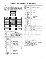
2. Installation
(1) Using desoldering braid, remove the solder from
the foil of each pin of the flat pack-IC on the CBA
so you can install a replacement flat pack-IC more
easily.
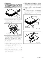
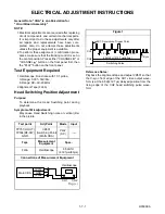
(2) The “
I
” mark on the flat pack-IC indicates pin 1.
(See Fig. S-1-7.) Be sure this mark matches the 1
on the PCB when positioning for installation. Then
presolder the four corners of the flat pack-IC. (See
Fig. S-1-8.)
(3) Solder all pins of the flat pack-IC. Be sure that none
of the pins have solder bridges.
Instructions for Handling
Semi-conductors
Electrostatic breakdown of the semi-conductors may
occur due to a potential difference caused by electro-
static charge during unpacking or repair work.
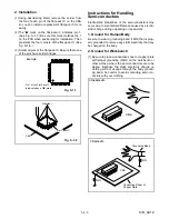
1. Ground for Human Body
Be sure to wear a grounding band (1M
Ω
) that is prop-
erly grounded to remove any static electricity that may
be charged on the body.
2. Ground for Workbench
(1) Be sure to place a conductive sheet or copper plate
with proper grounding (1M
Ω
) on the workbench or
other surface, where the semi-conductors are to be
placed. Because the static electricity charge on
clothing will not escape through the body ground-
ing band, be careful to avoid contacting semi-con-
ductors with your clothing.
Example :
Pin 1 of the Flat Pack-IC
is indicated by a " " mark.
Fig. S-1-7
Presolder
CBA
Flat Pack-IC
Fig. S-1-8
CBA
< Incorrect >
CBA
Grounding Band
Conductive Sheet or
Copper Plate
1M
Ω
1M
Ω
< Correct >
Содержание DCVR-4800
Страница 29: ...Main 1 9 Schematic Diagram VCR Section 1 10 3 1 10 4 H9512SCM1...
Страница 31: ...1 10 7 1 10 8 H9512SCM3 Main 3 9 Schematic Diagram VCR Section...
Страница 32: ...Main 4 9 Schematic Diagram VCR Section 1 10 9 1 10 10 H9512SCM4...
Страница 33: ...Main 5 9 Schematic Diagram VCR Section 1 10 11 1 10 12 H9512SCM5...
Страница 34: ...Main 6 9 Schematic Diagram VCR Section 1 10 13 1 10 14 H9512SCM6...
Страница 35: ...Main 7 9 Schematic Diagram VCR Section 1 10 15 1 10 16 H9512SCM7...
Страница 36: ...Main 8 9 DVD Open Close Schematic Diagram VCR Section 1 10 17 1 10 18 H9512SCM8...
Страница 37: ...1 10 19 1 10 20 Main 9 9 Schematic Diagram VCR Section H9512SCM9...
Страница 39: ...1 10 23 1 10 24 Jack Schematic Diagram VCR Section H9512SCJ...
Страница 40: ...1 10 25 1 10 26 Function Schematic Diagram VCR Section H9512SCF...
Страница 41: ...1 10 27 1 10 28 AFV Schematic Diagram VCR Section H9512SCAFV...
Страница 43: ...1 10 31 Main CBA Bottom View BH9510F01012A 1 10 32...
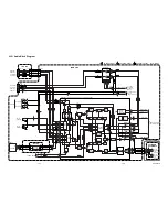
Страница 47: ...DVD Main 1 3 Schematic Diagram DVD Section H9512SCD1 1 10 39 1 10 40...
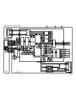
Страница 48: ...1 10 41 1 10 42 DVD Main 2 3 Schematic Diagram DVD Section H9512SCD2...
Страница 50: ...DVD Main 3 3 Schematic Diagram DVD Section 1 10 45 1 10 46 H9512SCD3...
Страница 77: ...3 1 3 H9512PEX S1 FRONT A14 X20 Some Ref Numbers are not in sequence X2 X3 X4 X1 Unit S3 S2 S2 X5 S7 Packing...
Страница 97: ...DCVR 4800 H9512FD...