MB95630H Series
528
FUJITSU SEMICONDUCTOR LIMITED
MN702-00009-1v0-E
CHAPTER 24 I
2
C BUS INTERFACE
24.8 Notes on Using I
2
C Bus Interface
24.8
Notes on Using I
2
C Bus Interface
This section provides notes on using the I
2
C bus interface.
■
Notes on Using I
2
C Bus Interface
●
Notes on setting I
2
C bus interface registers
•
Enable the I
2
C bus interface operation (ICCRn:EN) before setting the I
2
C bus control
registers (IBCR0n and IBCR1n).
•
Setting the master/slave select bit (IBCR1n:MSS) to "1" starts data transfer.
●
Notes on setting the shift clock frequency
•
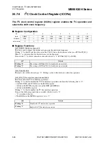
The shift clock frequency can be calculated by determining the m, n, and DMBP values
using the Fsck equation. See "24.7.6 I
C Clock Control Register (ICCRn)" for details of the
Fsck equation.
•
Do not write "1" to the DMBP bit in the ICCRn register if the value of n is 4
(ICCRn:CS[2:0] = 000).
●
Notes on priority for simultaneous write operations
•
Conflict between next byte transfer and stop condition
When writing "0" to IBCR1n:MSS and clearing IBCR1n:INT occur simultaneously, the
MSS bit is given priority and a STOP condition is generated.
•
Conflict between next byte transfer and start condition
When writing "1" to IBCR1n:SCC and clearing IBCR1n:INT occur simultaneously, the
SCC bit is given priority and a START condition is generated.
●
Notes on setting up using software
•
Do not select the repeated START condition (IBCR1n:SCC = 1) or slave mode
(IBCR1n:MSS = 0) simultaneously.
•
The I
2
C bus interface cannot return from interrupt processing if an interrupt request enable
bit is enabled (IBCR1n:BEIE = 1 or IBCR1n:INTE = 1) with the interrupt request flag bit
(IBCR1n:BER or IBCR1n:INT) set to "1". Clear the BER bit or the INT bit.
•
The following bits are cleared to "0" when the I
2
C bus interface operation is disabled
(ICCRn:EN = 0).
- AACKX, INTS, and WUE bits in the IBCR0n register
- All bits in the IBCR1n register except the BER bit and the BEIE bit
- All bits in the IBSRn register
●
Notes on data acknowledgment
In slave mode, a data acknowledge is generated if one of the following conditions is satisfied.
- The received address matches the value in the address register (IAARn) and
IBCR0n:AACKX is "0".
- A general call address (0x00) is received and IBCR1n:GACKE is "1".
Содержание MB95630H Series
Страница 2: ......
Страница 4: ......
Страница 8: ...iv ...
Страница 20: ...xvi ...
Страница 106: ...MB95630H Series 86 FUJITSU SEMICONDUCTOR LIMITED MN702 00009 1v0 E CHAPTER 6 I O PORT 6 2 Configuration and Operations ...
Страница 282: ...MB95630H Series 262 FUJITSU SEMICONDUCTOR LIMITED MN702 00009 1v0 E CHAPTER 14 LIN UART 14 8 Notes on Using LIN UART ...
Страница 642: ...MB95630H Series 622 FUJITSU SEMICONDUCTOR LIMITED MN702 00009 1v0 E APPENDIX A Instruction Overview A 5 Instruction Map ...
Страница 644: ......

