


MPC5553/MPC5554 Microcontroller Reference Manual, Rev. 5
9-32
Freescale Semiconductor
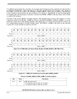
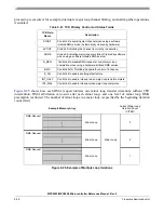
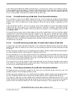
9.4.2
eDMA Basic Data Flow
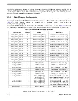
The basic flow of a data transfer can be partitioned into three segments. As shown in
, the first
segment involves the channel service request. In the diagram, this example uses the assertion of the eDMA
peripheral request signal to request service for channel
n
. Channel service request via software and the
TCDn.START bit follows the same basic flow as an eDMA peripheral request. The eDMA peripheral
request input signal is registered internally and then routed to through the eDMA engine, first through the
control module, then into the program model/channel arbitration module. In the next cycle, the channel
arbitration is performed, either using the fixed-priority or round-robin algorithm. After the arbitration is
complete, the activated channel number is sent through the address path and converted into the required
address to access the TCD local memory. Next, the TCD memory is accessed and the required descriptor
read from the local memory and loaded into the eDMA engine address path channel{x,y} registers. The
TCD memory is organized 64-bits in width to minimize the time needed to fetch the activated channel’s
descriptor and load it into the eDMA engine address path channel{x,y} registers.
Figure 9-22. eDMA Operation, Part 1
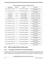
In the second part of the basic data flow as shown in
, the modules associated with the data
transfer (address path, data path and control) sequence through the required source reads and destination
writes to perform the actual data movement. The source reads are initiated and the fetched data is
temporarily stored in the data path module until it is gated onto the system bus during the destination write.
Slave Interfa
c
e
eDMA
eDMA Peripheral Request
System Bus
Data Path
Control
Address
Program Model/
Slave Write Data
Slave Write Address
Bus Write Data
Slave Read Data
Bus Address
eDMA Engine
TCD0
TCD
n
-1*
eDMA Interrupt Request
Bus Read Data
Channel Arbitration
eDMA Done Handshake
Path
SRAM
Transfer Control Descriptor
(TCD)
SRAM
*
n
= 64 channels in MPC5554
32 channels in MPC5553
Содержание MPC5553
Страница 5: ...MPC5553 MPC5554 Microcontroller Reference Manual Rev 5 2 Freescale Semiconductor...
Страница 21: ...MPC5553 MPC5554 Microcontroller Reference Manual Rev 5 xvi Freescale Semiconductor...
Страница 47: ...MPC5553 MPC5554 Microcontroller Reference Manual Rev 5 1 26 Freescale Semiconductor...
Страница 163: ...MPC5553 MPC5554 Microcontroller Reference Manual Rev 5 4 20 Freescale Semiconductor...
Страница 179: ...MPC5553 MPC5554 Microcontroller Reference Manual Rev 5 5 16 Freescale Semiconductor...
Страница 561: ...MPC5553 MPC5554 Microcontroller Reference Manual Rev 5 13 38 Freescale Semiconductor...
Страница 615: ...MPC5553 MPC5554 Microcontroller Reference Manual Rev 5 14 54 Freescale Semiconductor...
Страница 707: ...MPC5553 MPC5554 Microcontroller Reference Manual Rev 5 17 68 Freescale Semiconductor...
Страница 755: ...MPC5553 MPC5554 Microcontroller Reference Manual Rev 5 18 48 Freescale Semiconductor...
Страница 873: ...MPC5553 MPC5554 Microcontroller Reference Manual Rev 5 19 118 Freescale Semiconductor...
Страница 984: ...MPC5553 MPC5554 Microcontroller Reference Manual Rev 5 Freescale Semiconductor 21 41...
Страница 985: ...MPC5553 MPC5554 Microcontroller Reference Manual Rev 5 21 42 Freescale Semiconductor...
Страница 1019: ...MPC5553 MPC5554 Microcontroller Reference Manual Rev 5 22 34 Freescale Semiconductor...
Страница 1129: ...MPC5553 MPC5554 Microcontroller Reference Manual Rev 5 25 90 Freescale Semiconductor...
Страница 1207: ...Revision History 4 Freescale Semiconductor...


