


Hardware Description
Designer Reference Manual
DRM047 — Rev 0
32
Hardware Description
MOTOROLA
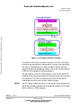
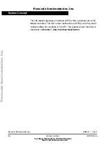
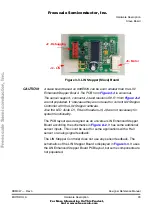
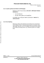
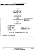
3.2.3 Software Download and Debugging
Connector J2 is used for software download or debugging. This is based
on so called MON08 mode (see
, Section 10
Monitor ROM)
The signals PTB4/AD4, PTB3/AD3, PTA1/KB1, PTA0/KB0, IRQ_IN
must be set according to
to put the MCU into MON08 mode
for software download or debugging (see
).
RST is the MCU reset pin. The MON08 mode must be timed with
external clock - PTC4/OSC.
There must be 9V for debugging on the IRQ_IN pin. Therefore the
jumper JP1 must be open. In user (standard operational) mode the
IRQ_IN must be attached to the IRQ_OUT from the Power Die module.
This is used for some operations like wake-up condition, where the
Power Die module. Therefore JP1 must be closed for user (standard
operational) mode.
Pin1 PTC4/OSC is precise clock input for MON08 mode. There must be
external clock source for the software download and debugging.
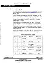
Table 3-1. Connector J2 Signals
Pin No
Input/
Output
Pin Name
Description
MON08 mode
1
PTC4/OSC
19,6608kHz
2
VSS
Ground
GND
3
VDD
5V supply
5V
4
In
IRQ_IN
MCU IRQ Input
9V
5
Out
IRQ_RQ
Power Die IRQ
output
jumper JP1 open
6
In
RST
MCU Reset input
falling edge
7
In/Out
PTA0/KB0
MON08 mode
serial
communication
19.200 kBaud
8
In
PTA1/KB1
MON08 mode
GND
9
In
PTB3/AD3
MON08 mode
GND
F
re
e
sc
a
le
S
e
m
ic
o
n
d
u
c
to
r,
I
Freescale Semiconductor, Inc.
For More Information On This Product,
Go to: www.freescale.com
n
c
.
..