


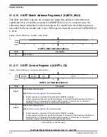


31.2.10 UART Match Address Registers 2 (UARTx_MA2)
The MA1 and MA2 registers are compared to input data addresses when the most
significant bit is set and the associated C4[MAEN] bit is set. If a match occurs, the
following data is transferred to the data register. If a match fails, the following data is
discarded. Software should only write a MA register when the associated C4[MAEN] bit
is clear.
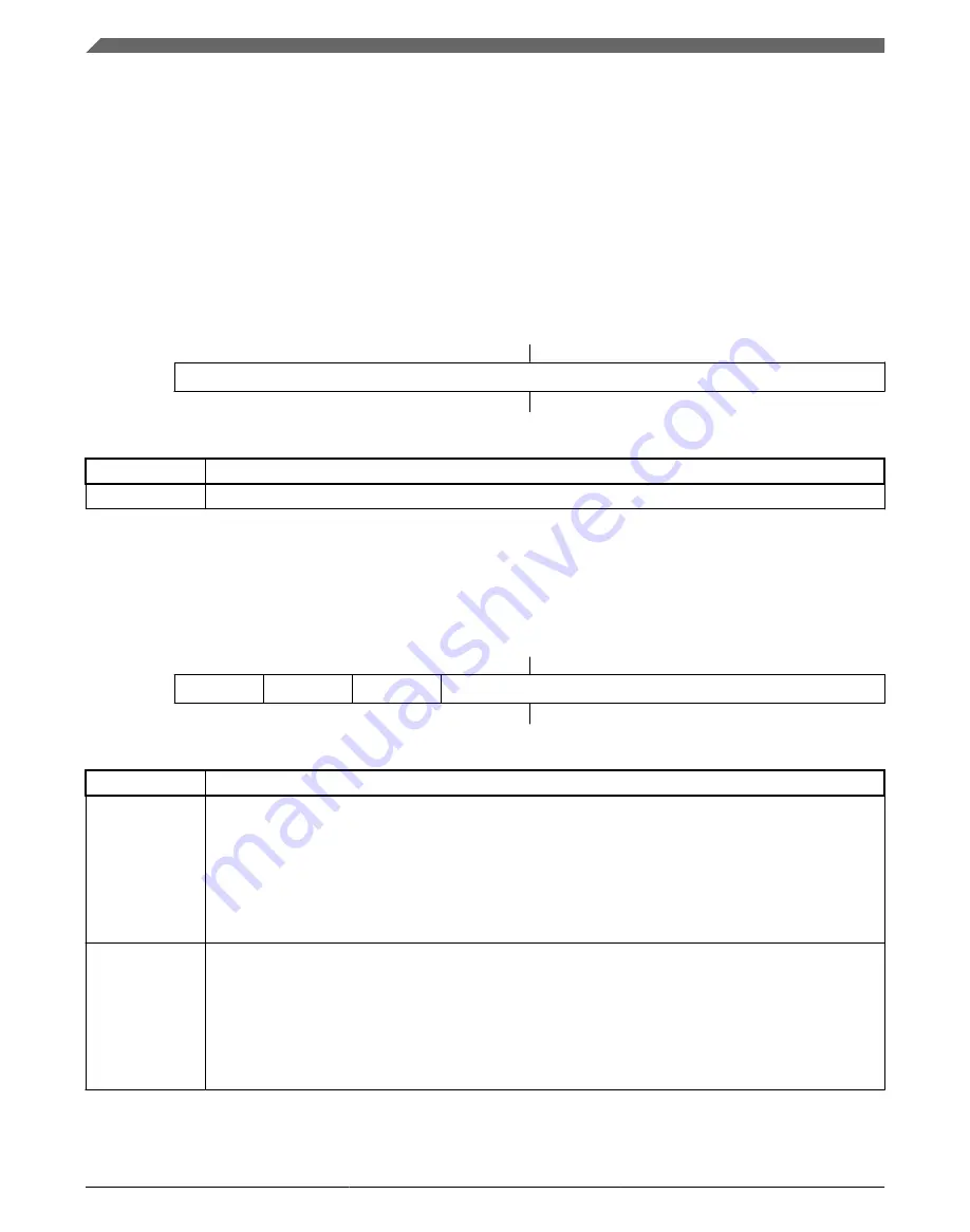
Address: 4006_A000h base + 9h offset = 4006_A009h
Bit
7
6
5
4
3
2
1
0
Read
Write
Reset
0
0
0
0
0
0
0
0
UARTx_MA2 field descriptions
Field
Description
MA
Match Address
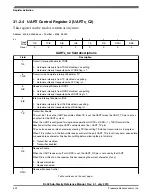
31.2.11 UART Control Register 4 (UARTx_C4)
Address: 4006_A000h base + Ah offset = 4006_A00Ah
Bit
7
6
5
4
3
2
1
0
Read
Write
Reset
0
0
0
0
1
1
1
1
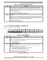
UARTx_C4 field descriptions
Field
Description
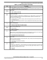
7
MAEN1
Match Address Mode Enable 1
Refer to
for more information.
0
All data received is transferred to the data buffer if MAEN2 is cleared.
1
All data received with the most significant bit cleared, is discarded. All data received with the most
significant bit set, is compared with contents of MA1 register. If no match occurs, the data is
discarded. If match occurs, data is transferred to the data buffer.
6
MAEN2
Match Address Mode Enable 2
Refer to
for more information.
0
All data received is transferred to the data buffer if MAEN1 is cleared.
1
All data received with the most significant bit cleared, is discarded. All data received with the most
significant bit set, is compared with contents of MA2 register. If no match occurs, the data is
discarded. If match occurs, data is transferred to the data buffer.
Table continues on the next page...
Register definition
KL02 Sub-Family Reference Manual, Rev. 2.1, July 2013
510
Freescale Semiconductor, Inc.
Содержание KKL02Z32CAF4R
Страница 2: ...KL02 Sub Family Reference Manual Rev 2 1 July 2013 2 Freescale Semiconductor Inc...
Страница 24: ...KL02 Sub Family Reference Manual Rev 2 1 July 2013 24 Freescale Semiconductor Inc...
Страница 36: ...Orderable part numbers KL02 Sub Family Reference Manual Rev 2 1 July 2013 36 Freescale Semiconductor Inc...
Страница 76: ...Human machine interfaces HMI KL02 Sub Family Reference Manual Rev 2 1 July 2013 76 Freescale Semiconductor Inc...
Страница 94: ...Module clocks KL02 Sub Family Reference Manual Rev 2 1 July 2013 94 Freescale Semiconductor Inc...
Страница 142: ...Functional description KL02 Sub Family Reference Manual Rev 2 1 July 2013 142 Freescale Semiconductor Inc...
Страница 188: ...Memory map and register descriptions KL02 Sub Family Reference Manual Rev 2 1 July 2013 188 Freescale Semiconductor Inc...
Страница 214: ...Application information KL02 Sub Family Reference Manual Rev 2 1 July 2013 214 Freescale Semiconductor Inc...
Страница 222: ...Memory map register descriptions KL02 Sub Family Reference Manual Rev 2 1 July 2013 222 Freescale Semiconductor Inc...
Страница 256: ...Memory map and register definition KL02 Sub Family Reference Manual Rev 2 1 July 2013 256 Freescale Semiconductor Inc...
Страница 300: ...Functional description KL02 Sub Family Reference Manual Rev 2 1 July 2013 300 Freescale Semiconductor Inc...
Страница 532: ...Functional description KL02 Sub Family Reference Manual Rev 2 1 July 2013 532 Freescale Semiconductor Inc...
Страница 534: ...KL02 Sub Family Reference Manual Rev 2 1 July 2013 534 Freescale Semiconductor Inc...


