


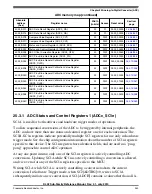
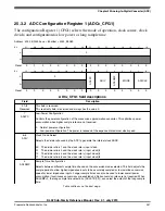
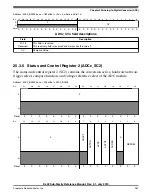
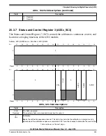
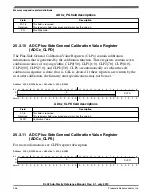
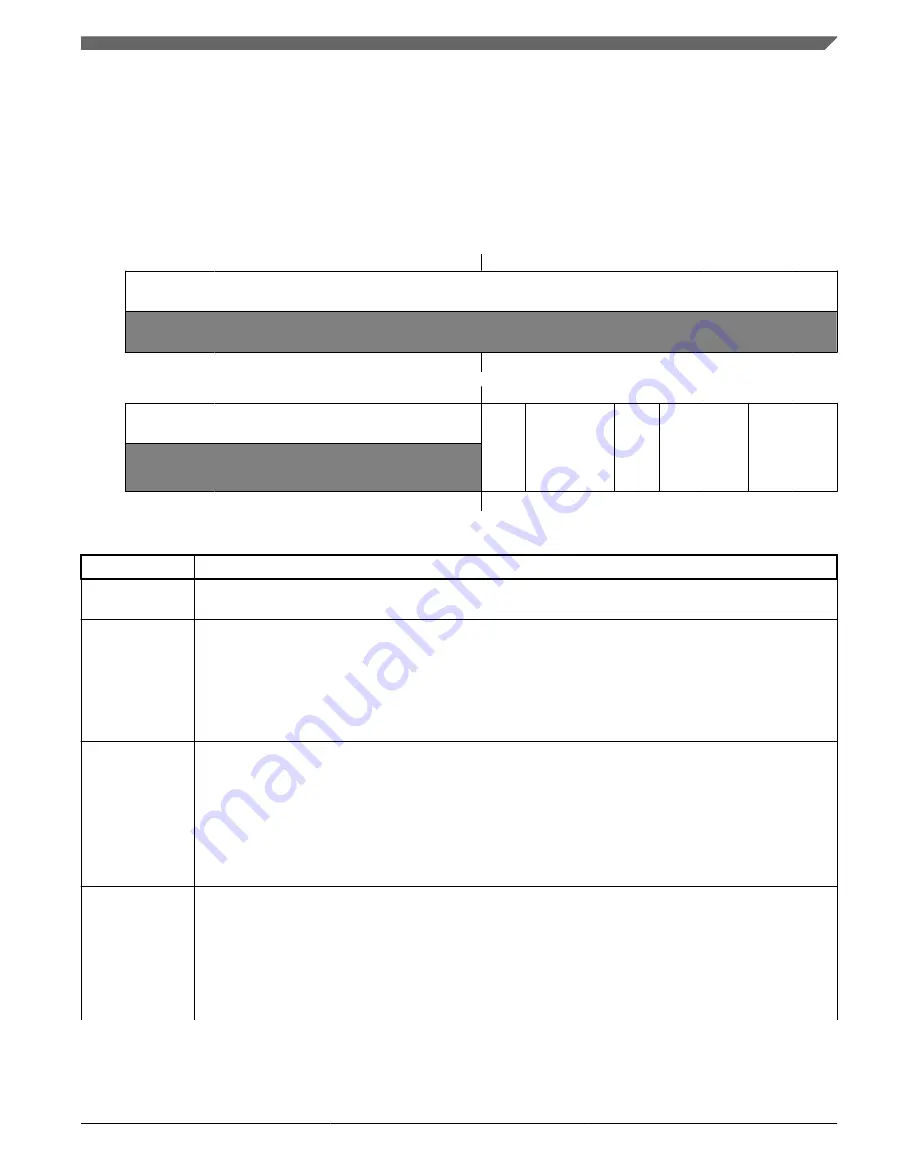
25.3.2 ADC Configuration Register 1 (ADCx_CFG1)
The configuration Register 1 (CFG1) selects the mode of operation, clock source, clock
divide, and configuration for low power or long sample time.
Address: 4003_B000h base + 8h offset = 4003_B008h
Bit
31
30
29
28
27
26
25
24
23
22
21
20
19
18
17
16
R
W
Reset
0
0
0
0
0
0
0
0
0
0
0
0
0
0
0
0
Bit
15
14
13
12
11
10
9
8
7
6
5
4
3
2
1
0
R
W
Reset
0
0
0
0
0
0
0
0
0
0
0
0
0
0
0
0
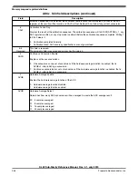
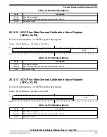
ADCx_CFG1 field descriptions
Field
Description
31–8
Reserved
This field is reserved.
This read-only field is reserved and always has the value 0.
7
ADLPC
Low-Power Configuration
Controls the power configuration of the successive approximation converter. This optimizes power
consumption when higher sample rates are not required.
0
Normal power configuration.
1
Low-power configuration. The power is reduced at the expense of maximum clock speed.
6–5
ADIV
Clock Divide Select
Selects the divide ratio used by the ADC to generate the internal clock ADCK.
00
The divide ratio is 1 and the clock rate is input clock.
01
The divide ratio is 2 and the clock rate is (input clock)/2.
10
The divide ratio is 4 and the clock rate is (input clock)/4.
11
The divide ratio is 8 and the clock rate is (input clock)/8.
4
ADLSMP
Sample Time Configuration
Selects between different sample times based on the conversion mode selected. This field adjusts the
sample period to allow higher impedance inputs to be accurately sampled or to maximize conversion
speed for lower impedance inputs. Longer sample times can also be used to lower overall power
consumption if continuous conversions are enabled and high conversion rates are not required. When
ADLSMP=1, the long sample time select bits, (ADLSTS[1:0]), can select the extent of the long sample
time.
Table continues on the next page...
Chapter 25 Analog-to-Digital Converter (ADC)
KL02 Sub-Family Reference Manual, Rev. 2.1, July 2013
Freescale Semiconductor, Inc.
347
Содержание KKL02Z32CAF4R
Страница 2: ...KL02 Sub Family Reference Manual Rev 2 1 July 2013 2 Freescale Semiconductor Inc...
Страница 24: ...KL02 Sub Family Reference Manual Rev 2 1 July 2013 24 Freescale Semiconductor Inc...
Страница 36: ...Orderable part numbers KL02 Sub Family Reference Manual Rev 2 1 July 2013 36 Freescale Semiconductor Inc...
Страница 76: ...Human machine interfaces HMI KL02 Sub Family Reference Manual Rev 2 1 July 2013 76 Freescale Semiconductor Inc...
Страница 94: ...Module clocks KL02 Sub Family Reference Manual Rev 2 1 July 2013 94 Freescale Semiconductor Inc...
Страница 142: ...Functional description KL02 Sub Family Reference Manual Rev 2 1 July 2013 142 Freescale Semiconductor Inc...
Страница 188: ...Memory map and register descriptions KL02 Sub Family Reference Manual Rev 2 1 July 2013 188 Freescale Semiconductor Inc...
Страница 214: ...Application information KL02 Sub Family Reference Manual Rev 2 1 July 2013 214 Freescale Semiconductor Inc...
Страница 222: ...Memory map register descriptions KL02 Sub Family Reference Manual Rev 2 1 July 2013 222 Freescale Semiconductor Inc...
Страница 256: ...Memory map and register definition KL02 Sub Family Reference Manual Rev 2 1 July 2013 256 Freescale Semiconductor Inc...
Страница 300: ...Functional description KL02 Sub Family Reference Manual Rev 2 1 July 2013 300 Freescale Semiconductor Inc...
Страница 532: ...Functional description KL02 Sub Family Reference Manual Rev 2 1 July 2013 532 Freescale Semiconductor Inc...
Страница 534: ...KL02 Sub Family Reference Manual Rev 2 1 July 2013 534 Freescale Semiconductor Inc...


