


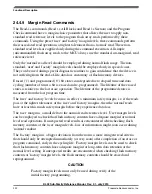


CAUTION
A flash memory location must be in the erased state before
being programmed. Cumulative programming of bits (back-to-
back program operations without an intervening erase) within a
flash memory location is not allowed. Re-programming of
existing 0s to 0 is not allowed as this overstresses the device.
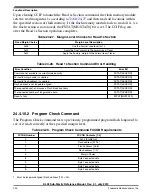
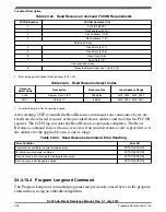
Table 24-35. Program Longword Command FCCOB Requirements
FCCOB Number
FCCOB Contents [7:0]
0
0x06 (PGM4)
1
Flash address [23:16]
2
Flash address [15:8]
3
4
Byte 0 program value
5
Byte 1 program value
6
Byte 2 program value
7
Byte 3 program value
1. Must be longword aligned (Flash address [1:0] = 00).
Upon clearing CCIF to launch the Program Longword command, the flash memory
module programs the data bytes into the flash using the supplied address. The targeted
flash locations must be currently unprotected (see the description of the FPROT registers)
to permit execution of the Program Longword operation.
The programming operation is unidirectional. It can only move NVM bits from the erased
state ('1') to the programmed state ('0'). Erased bits that fail to program to the '0' state are
flagged as errors in FSTAT[MGSTAT0]. The CCIF flag is set after the Program
Longword operation completes.
The supplied address must be longword aligned (flash address [1:0] = 00):
• Byte 3 data is written to the supplied byte address ('start'),
• Byte 2 data is programmed to byte address start+0b01,
• Byte 1 data is programmed to byte address start+0b10, and
• Byte 0 data is programmed to byte address start+0b11.
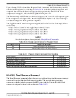
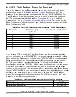
Table 24-36. Program Longword Command Error Handling
Error Condition
Error Bit
Command not available in current mode/security
FSTAT[ACCERR]
An invalid flash address is supplied
FSTAT[ACCERR]
Flash address is not longword aligned
FSTAT[ACCERR]
Flash address points to a protected area
FSTAT[FPVIOL]
Table continues on the next page...
Chapter 24 Flash Memory Module (FTFA)
KL02 Sub-Family Reference Manual, Rev. 2.1, July 2013
Freescale Semiconductor, Inc.
327
Содержание KKL02Z32CAF4R
Страница 2: ...KL02 Sub Family Reference Manual Rev 2 1 July 2013 2 Freescale Semiconductor Inc...
Страница 24: ...KL02 Sub Family Reference Manual Rev 2 1 July 2013 24 Freescale Semiconductor Inc...
Страница 36: ...Orderable part numbers KL02 Sub Family Reference Manual Rev 2 1 July 2013 36 Freescale Semiconductor Inc...
Страница 76: ...Human machine interfaces HMI KL02 Sub Family Reference Manual Rev 2 1 July 2013 76 Freescale Semiconductor Inc...
Страница 94: ...Module clocks KL02 Sub Family Reference Manual Rev 2 1 July 2013 94 Freescale Semiconductor Inc...
Страница 142: ...Functional description KL02 Sub Family Reference Manual Rev 2 1 July 2013 142 Freescale Semiconductor Inc...
Страница 188: ...Memory map and register descriptions KL02 Sub Family Reference Manual Rev 2 1 July 2013 188 Freescale Semiconductor Inc...
Страница 214: ...Application information KL02 Sub Family Reference Manual Rev 2 1 July 2013 214 Freescale Semiconductor Inc...
Страница 222: ...Memory map register descriptions KL02 Sub Family Reference Manual Rev 2 1 July 2013 222 Freescale Semiconductor Inc...
Страница 256: ...Memory map and register definition KL02 Sub Family Reference Manual Rev 2 1 July 2013 256 Freescale Semiconductor Inc...
Страница 300: ...Functional description KL02 Sub Family Reference Manual Rev 2 1 July 2013 300 Freescale Semiconductor Inc...
Страница 532: ...Functional description KL02 Sub Family Reference Manual Rev 2 1 July 2013 532 Freescale Semiconductor Inc...
Страница 534: ...KL02 Sub Family Reference Manual Rev 2 1 July 2013 534 Freescale Semiconductor Inc...


