Fibocom L830-EB-11 Скачать руководство пользователя страница 28

Reproduction forbidden without Fibocom Wireless Inc. written authorization - All Rights Reserved.

L830-EB-11 Hardware User Manual

Page 25 of 39

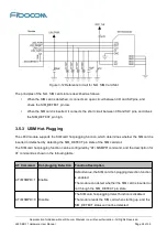
After the SIM card hot-plugging detection function is enabled, the module detects that the SIM card is
inserted when the SIM_DETECT pin is high, then executes the initialization program and finish the
network registration after reading the SIM card information. When the SIM_DETECT pin is low, the
module determines that the SIM card is detached and does not read the SIM card.

Note:

By default, SIM_DETECT is active-high, which can be switched to active-low by the AT
command. Please refer to the AT Commands Manual for the AT command.
The system doesn

t need SIM hot-plug function, please left SIM_DTECT floating.

3.5.4 USIM Design

The SIM card circuit design shall meet the EMC standards and ESD requirements with the improved
capability to resist interference, to ensure that the SIM card can work stably. The following guidelines
should be noted in case of design:

The SIM card slot placement should near the module as close as possible, and away from the
RF antenna, DC/DC power supply, clock signal lines, and other strong interference sources.

The SIM card slot with a metal shielding housing can improve the anti-interference ability.

The trace length between the SIM card slot and the module should not exceed 100mm, or it
could reduce the signal quality.

The UIM_CLK and UIM_DATA signal lines should be isolated by GND to avoid crosstalk
interference. If it is difficult for the layout, the whole SIM signal lines should be wrapped with
GND as a group at least.

The filter capacitors and ESD devices for SIM card signals should be placed near to the SIM
card slot, and the ESD devices with 22~33pF capacitance should be used.

3.6

Status Indicator

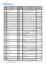
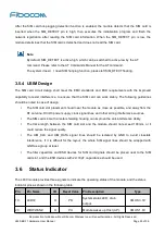
The L830 module provides three signals to indicate the operating status of the module, and the status
indicator pins as shown in the following table:

Pin

Pin Name

I/O

Reset Value Pin Description

Type

10

LED1#

O

PD

System status LED, drain
output.

CMOS 3.3V

23

WOWWAN#

O

PU

Module wakes up Host (AP).

CMOS 1.8V

Содержание L830-EB-11

Страница 1: ...production forbidden without Fibocom Wireless Inc written authorization All Rights Reserved L830 EBHardware User Manual Page 1 of 39 L830 EB 11 Hardware User Manual Version V1 0 2 Update date 2017 09...

Страница 2: ...production forbidden without Fibocom Wireless Inc written authorization All Rights Reserved L830 EB 11 Hardware User Manual Page 2 of 39 Applicability Table No Product model Description 1 L830 EB 11 N...

Страница 3: ...re document or distribute the document in any form Notice The document is subject to update from time to time owing to the product version upgrade or other reasons Unless otherwise specified the docum...

Страница 4: ...3 1 M 2 Interface 9 3 1 1 Pin Map 10 3 1 2 Pin Definition 11 3 2 Power Supply 14 3 2 1 Power Supply 15 3 2 2 Logic level 16 3 2 3 Power Consumption 16 3 3 Control Signal 17 3 3 1 Module Start Up 17 3...

Страница 5: ...on 29 3 10 Clock Interface 30 3 11 Configuration Interface 30 3 12 Other Interfaces 31 4 Radio Frequency 31 4 1 RF Interface 31 4 1 1 RF Interface Functionality 31 4 1 2 RF Connector Characteristic 31...

Страница 6: ...1 Conformance specification 3GPP TS 36 521 1 V10 6 0 User Equipment UE conformance specification Radio transmission and reception Part 1 Conformance testing 3GPP TS 21 111 V10 0 0 USIM and IC card re...

Страница 7: ...bility and that this product Product description LTE module Type designation s L830 EB 11 Trademark Fibocom Product Identification Element L830 EB 11 is in conformity with the relevant Union harmoniza...

Страница 8: ...use harmful interference to radio communications However there is no guarantee that interference will not occur in a particular installation If this equipment does cause harmful interference to radio...

Страница 9: ...ble for re evaluating the end product including the transmitter and obtaining a separate FCC authorization End Product Labeling This transmitter module is authorized only for use in device where the a...

Страница 10: ...nd I VIII GPS GLONASS Not Support CA LTE inter band CA 1 3 7 20 3 7 8 20 28 32 7 20 28 LTE intra band CA 3 7 Data Transmission LTE FDD 300Mbps DL 50Mbps UL Cat 6 UMTS HSPA UMTS 384 kbps DL 384 kbps UL...

Страница 11: ...e Protocol Stack IPV4 IPV6 AT commands 3GPP TS 27 007 and 27 005 and proprietary FIBOCOM AT commands Firmware update USB Note When temperature goes beyond normal operating temperature range of 10 C 55...

Страница 12: ...e functions of L830 module including baseband and RF functions Baseband contains the followings UMTS LTE FDD controller Power supply NAND internal LPDDR2 RAM Application interface RF contains the foll...

Страница 13: ...forbidden without Fibocom Wireless Inc written authorization All Rights Reserved L830 EB 11 Hardware User Manual Page 10 of 39 3 1 1 Pin Map Figure 3 1 Pin Map Note Pin Notch represents the gap of the...

Страница 14: ...ain power input Power Supply 5 GND GND Power Supply 6 FULL_CARD_POWER_OFF I Power on off control signal active High CMOS 3 3 1 8V 7 USB D I O USB 2 0 D signal 0 3 3V 8 W_DISABLE1 I PU WWAN Disable act...

Страница 15: ...ly 28 I2S_WA O PD I2S clock for left and right channels CMOS 1 8V 29 NC NC 30 UIM_RESET O PP USIM reset signal 1 8V 3V 31 NC NC 32 UIM_CLK O PP USIM clock signal 1 8V 3V 33 GND GND Power Supply 34 UIM...

Страница 16: ...TCTL0 O L Tunable antenna control signal bit0 not supported yet CMOS 1 8V 60 COEX3 O Reserved 61 ANTCTL1 O L Tunable antenna control signal MIPI RFFE SDATA bit1 not supported yet CMOS 1 8V 62 COEX2 O...

Страница 17: ...Supply 75 CONFIG_2 O L Connected to internal GND L830 M 2 module is configured as the WWAN SSIC 0 interface type Reset Value The initial status after module reset not the status when working H High Vo...

Страница 18: ...uires the capacitor of no less than 220uF The capacitor for battery power supply can be reduced to 100uF 1uF 100nF Digital signal noise Filter out the interference generated from the clock and digital...

Страница 19: ...logic level 1 71 1 8 1 89 V VIH 1 3 1 8 1 89 V VIL 0 3 0 0 3 V The L830 module 3 3V logic level definition as shown in the following table Parameters Minimum Typical Maximum Unit 3 3V logic level 3 1...

Страница 20: ...Bm 675 LTE FDD Data transfer Band 20 23dBm 685 LTE FDD Data transfer Band 28 23dBm 833 Note The data above is an average value obtained by testing some samples 3 3 Control Signal The L830 module provi...

Страница 21: ...circuit design is shown in Figure 3 5 Figure 3 4 Circuit for Module Start up Controlled by AP Figure 3 5 Circuit for Automatic Start up 3 3 1 2 Start up Timing Sequence After powering on module will s...

Страница 22: ...Condition Software Sending AT CFUN 0 command Normal shutdown Hardware Pull down FULL_CARD_POWER_OFF pin Only used when a hardware exception occurs and the software control cannot be used Module can b...

Страница 23: ...100ms The time difference between the RESET signal and the FULL_CARD_POWER_OFF signal 3 3 3 Module Reset The L830 module can reset to its initial status by pulling down the RESET signal for more than...

Страница 24: ...L830 module supports USB 2 0 which is compatible with USB High Speed 480 Mbit s and USB Full Speed 12 Mbit s For the USB timing and electrical specification of L830 module please refer to Universal S...

Страница 25: ...lly in the case of PCB layout USB_D and USB_D signal lines should have the differential impedance of 90 ohms USB_D and USB_D signal lines should be parallel and have the equal length the right angle r...

Страница 26: ...5 2 1 N C SIM Card Slot The reference circuit design for N C Normally Closed SIM card slot is shown in Figure 3 11 Figure 3 11 Reference Circuit for N C SIM Card Slot The principles of the N C SIM car...

Страница 27: ...30 module supports the SIM card hot plugging function which determines whether the SIM card is inserted or detached by detecting the SIM_DETECT pin state of the SIM card slot The SIM card hot plugging...

Страница 28: ...The following guidelines should be noted in case of design The SIM card slot placement should near the module as close as possible and away from the RF antenna DC DC power supply clock signal lines a...

Страница 29: ...ED On RF function OFF High level LED Off The LED driving circuit is shown in figure 3 13 Figure 3 13 LED Driving Circuit Note The resistance of LED current limiting resistor is selected according to t...

Страница 30: ...pe 8 W_DISABLE1 I PU Enable Disable RF network CMOS 3 3V 25 DPR I PU Body SAR detection CMOS 1 8V 3 7 1 W_DISABLE1 The module provides a hardware pin to enable disable WWAN RF function and the functio...

Страница 31: ...m emission power to the threshold value of the module 3 8 Digital Audio The L830 module supports I2S digital audio interface and it supports the ordinary I2S mode and PCM mode The signal level of the...

Страница 32: ...19 Signal Connection for PCM Mode Description The PCM mode interface can be configured as master or slave mode It supports various audio sampling rates 444 1KHz 32KHz 24KHz 16KHz 8KHz It supports shor...

Страница 33: ...clock interface it can output 26MHz clock Pin Pin Name I O Reset Value Pin Description Type 46 SYSCLK O 26MHz clock output can be used for external GPS or Audio Codec 1 8V 3 11 Configuration Interface...

Страница 34: ...4 1 1 RF Interface Functionality The L830 module supports two RF connectors used for external antenna connection As the Figure 4 1 shows M is for Main antenna used to receive and transmit RF signals D...

Страница 35: ...ension The L830 module adopts standard M 2 module RF connectors the model name is 818004607 from ETC company and the connector size is 2 2 0 6m The connector dimension is shown as following picture Fi...

Страница 36: ...D 703 748 758 803 Band 32 L Band1500 LTE FDD N A 1452 1496 4 3 Transmitting Power The transmitting power for each band of the L830 module as shown in the following table Mode Band 3GPP Requirement Tx...

Страница 37: ...l antennas situation Main Diversity For single main antenna without Diversity the sensitivity will drop around 3dBm for each band of LTE 4 5 GNSS L830 EB 11 module not support GNSS 4 6 Antenna Design...

Страница 38: ...dule Main antenna requirements Input power 25dBm average power WCDMA LTE Recommended standing wave ratio SWR 2 1 5 Structure Specification 5 1 Product Appearance The product appearance for L830 module...

Страница 39: ...ace Model The L830 M 2 module adopts 75 pin gold finger as external interface where 67 pins are signal pins and 8 pins are notch pins as shown in Figure 3 1 For module dimension please refer to chapte...

Страница 40: ...connector please refer to the specification Figure 5 3 M 2 Dimension of Structure 5 5 Storage 5 5 1 Storage Life Storage Conditions recommended Temperature is 23 5 relative humidity is RH 35 70 Stora...

Страница 41: ...e module is a precision electronic product and may suffer permanent damage if no correct electrostatic protection measures are taken 5 6 1 Tray Package The L830 module uses tray package 20 pcs are pac...

Страница 42: ...User Manual Page 39 of 39 5 6 2 Tray size The pallet size is 330 175 6 0mm as shown in Figure 5 5 ITEM L W H T A0 B0 DIM 330 0 0 5 175 0 0 5 6 0 0 3 0 5 0 1 43 0 3 33 0 0 3 ITEM A1 B1 C D E F DIM 294...

Отзывы: