background image

©2002 Fairchild Semiconductor Corporation

Application Note 7511 Rev. A1

.

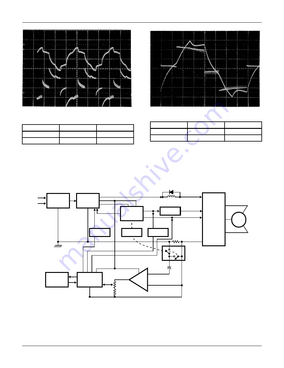
FIGURE 13A. MOTOR CURRENT AND VOLTAGE ARE SHOWN 

HERE, FOR LIGHT LOADS

FIGURE 13B. MOTOR CURRENT AND VOLTAGE ARE SHOWN 

HERE, FOR HEAVY LOADS.

To complete the design of the 6-step motor drive, it’s necessary to consider protection circuitry for the output IGTs. The drive receives its
power from a switching supply already containing provisions for protection from line over-voltage and under-voltage and transient effects.
However, you still have to guard the power switches against unwanted effects on the output lines and the possibility of noise or other
extraneous signals causing gate-drive timing errors.

The best protection circuit must match the characteristics of the power switch and the circuit’s bias conditions. The IGT is very rugged
during turn-on and conduction, but it requires time to dissipate minority carriers when turning off high currents and voltages. An analysis
of the possible malfunction condition

FIGURE 14. THE LOWEST COST SENSOR IMAGINABLE, A PIECE OF COPPER WIRE SERVES AS THE CURRENT MONITOR IN THIS SYS-

TEM. THE CHOPPED AND AMPLIFIED VOLTAGE DROP ACROSS THE WIRE TRIGGERS A GATE-DRIVE SHUT-OFF CIRCUIT
UNDER FAULT CONDITIONS.

TRACE

VERTICAL

HORIZONTAL

A

1A/DIV

1mSEC/DIV

B

50V/DIV

1mSEC/DIV

TRACE

VERTICAL

HORIZONTAL

A

3A/DIV

2mSEC/DIV

B

100V/DIV

2mSEC/DIV

AC

LINE

INPUT

HV

DISABLE

GATE DRIVE

TURNOFF

HV

ADJUST

50 TO 320V DC

5V DC

UPPER 3

LOWER 3

dI/dt LIMIT

24V DC

CHOPPER

I LIMIT

10A

20A

ISOLATION

ISOLATION

IGT

SWITCHES

MOTOR

CONTROL

AND

TIMING

ISOLATION

RECTIFIER

AND

FILTER

SWITCHING

POWER

SUPPLY

RECYCLE

TIME

COMPARATOR

AND LATCH

AC

AV = 100

ISOLATION

Application Note 7511

Содержание AN-7511

Страница 1: ... sum of R3 and the parallel combination of R1 and R2 sets the turn on time Drive circuit requirements however are more complex in the common collector configuration Figure 1B In this floating gate supply floating control drive scheme R1 controls the gate supply s power loss R2 governs the turn off time and the sum of R1 and R2 sets the turn on time Figure 1C shows another common collector configur...

Страница 2: ...ler drive along with its transient response In some applications the photovoltaic element can charge a storage capacitor that s subsequently switched with a phototransistor isolator This isolator technique similar to that used in bootstrap circuits provides rapid turn on and turn off while maintaining small size good isolation and low cost In common collector applications involving high voltage re...

Страница 3: ...NTROL INPUT ON OFF GFOE1A1 EMITTER DISCONNECTED DETECTOR CONNECTED 10M 30FT QSF2000C W CONNECTORS GFOD1A1 1N914 R1 2N5354 C Q1 R2 R3 IGT FIGURE 4 ELIMINATE EMI IN HIGH FLUX OR NOISE ENVI RONMENTS BY USING FIBER OPTIC COMPO NENTS THESE PARTS ALSO ALLEVIATE PROBLEMS ARISING FROM CAPACITIVE COU PLING IN ISOLATION ELEMENTS Piezos Pare Prices OUTPUT VOLTAGE ACOUSTIC WAVE OSCILLATOR IGT 4 7k 1N914 1N914...

Страница 4: ...GH ISOLATION AT LOW COST PULSE TRANSFORMERS ARE IDEAL FOR DRIVING THE IGT AT SUFFICIENTLY HIGH FREQUENCIES C1 CAN BE THE IGT S GATE EMITTERCAPACITANCE ALONE FIGURE 6B A HIGH FREQUENCY OSCILLATOR IN THE TRANS FORMER S PRIMARY YIELDS UNLIMITED ON TIME CAPABILITY In the pulse on pulse off method Figure 6A C1 stores a positive pulse holding the IGT on At moderate frequencies several hundred Hertz and ...

Страница 5: ...ransformer reasonably small The volt age doubler circuitry improves the turn on time and also pro vides long on time capability Although this design uses only a 5V supply on the primary side of a standard trigger trans former it provides 15V gate to emitter voltage FIGURE 7 THIS DRIVING METHOD FOR LOW FREQUENCY SWITCHING PROVIDES 15V TO THE IGT S GATE OSCILLATOR 1 2 1N914 0 001µF 4 7k 0 001 µF IGT...

Страница 6: ...r to shut off The inverter s power out put circuit is shown in Figure 9A the corresponding timing diagrams show resistive load current waveforms that indi cate the 3 phase power Figure 9B and waveforms of the out put line voltage and current Figure 9C In Figure 9 s circuit it appears that IGTs Q1 through Q6 will conduct for 180o However in a practical situation it s neces sary to provide some time...

Страница 7: ... could also do the job but the 500V choice gives an additional derating safety margin You must set the current limit at 9A to limit the in rush current during start up Note that thanks to the IGT s adequate RBSOA you don t need turn off snubbers FIGURE 11A PROVIDING PROPERLY TIMED DRIVE TO THE IGTS THE CIRCUIT USES PIEZO COUPLING TO THE UPPER POWER DEVICE THE 3 TRANSISTOR DELAY CIRCUIT PROVIDES TH...

Страница 8: ...65o Conduction Prevents Shoot Through Consider however using Figure 11A s novel low cost cir cuit It uses a piezo coupler to drive the isolated IGT As noted the coupler needs a high frequency square wave to induce mechanical oscillations in its primary side The 555 oscillator provides the necessary 108 kHz waveform its out put is gated according to the required timing logic and then applied to the...

Страница 9: ...f the power switch and the circuit s bias conditions The IGT is very rugged during turn on and conduction but it requires time to dissipate minority carriers when turning off high currents and voltages An analysis of the possible malfunction condition FIGURE 14 THE LOWEST COST SENSOR IMAGINABLE A PIECE OF COPPER WIRE SERVES AS THE CURRENT MONITOR IN THIS SYS TEM THE CHOPPED AND AMPLIFIED VOLTAGE D...

Страница 10: ...5V 5µF 25V 220k 2 2k 0 001 µF H11F3 H11F3 TO CONTROL CIRCUIT 39 470 pF 390 20A 2k 2mΩ 1 24 AWG COPPER POWER SUPPLY CURRENT SENSE AND CHOPPER AC AMPLIFIER LATCHING FAST COMPARATOR 10ms RESET IGT POWER SWITCHES A139M 50µH 10k 180k 47k 39k 0 001 µF 1k 2N5306 C203B 0 02 µF 22k H11AV2 TO PZO SHUTDOWN H11AV2 TO HI V SHUTDOWN 22 0 2µF 2 1 TO DRIVE DT230F TO MOTOR TIMER 555 1 3 CHOPPER DRIVE TO PIEZO DRIV...

Страница 11: ...ich the IGT latches on while in forward conduction is typically three to four times the device s maximum rated collector current When the collector current drops below the value that provokes Q2 turn on normal operation resumes if chip temperature is still within ratings If the gate to emitter resistance is too low the Q2 Q3 parasitic SCR can cause the IGT to latch up during turn off During this p...

Страница 12: ...EAT ER THAN THAT OF THE IGT S GATE DRIVE SO THE IGT UNDER TEST IS SWITCHED THROUGH Q1 WHEN REVERSE BIAS LATCH UP OCCURS PULSE GENERATOR PULSE GENERATOR TRIGGER 1000pF A114A A114A 1k 100 100 50 10 D38H1 D44D6 Q1 D66EV7 Q2 DUT D94FQ4 DS0026x2 5V 1N914 10V PE 63385 A114A 15V D66EV7 Q1 RGE 1 10k VCE A139M 10 VCC VCLAMP 400V MAX 0 02µF 10µF A139P L 100µH 2k Q2 Application Note 7511 ...

Страница 13: ...support device or system or to affect its safety or effectiveness PRODUCT STATUS DEFINITIONS Definition of Terms Datasheet Identification Product Status Definition Advance Information Preliminary No Identification Needed Obsolete This datasheet contains the design specifications for product development Specifications may change in any manner without notice This datasheet contains preliminary data ...

Отзывы: