background image

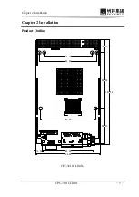
Chapter 2 Installation 

CPC­3811CLD4N 

-

  9 

-


Tip: How to identify the first pin of the jumpers and interfaces


1.  Observe  the  letter  beside  the  socket,  it  would  be  marked  with  “1”  or  thickened 

lines or triangular symbols; 

2.  Observe the solder pad on the back, the square pad is the first pin; 

3.  The red line on the cable or other marks shows that they should be connected with 

the first pin of the socket.


Instruction of CPC­3811CLD4N­1 

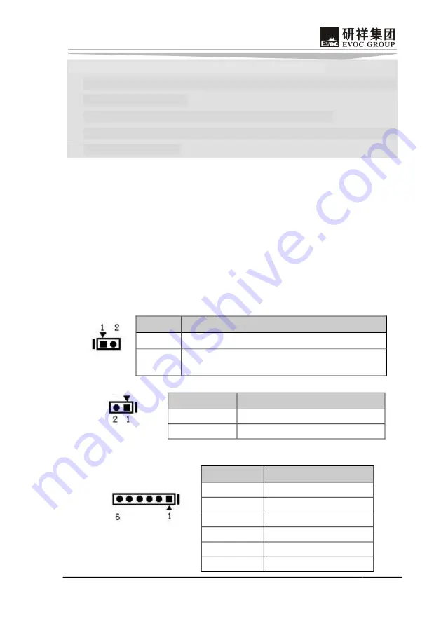
Jumper Setup 

(1) 

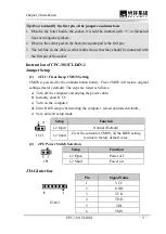
JCC1: Clear/Keep CMOS Setting


CMOS is powered by the onboard button battery. Clear CMOS will restore original 

settings (factory default). The steps are listed as follows: 

a)  Turn off the computer and unplug the power cable; 

b)  Instantly short JCC1; 

c)  Turn on the computer; 

d)  Enter BIOS setup when starting the computer, reload optimized defaults; 

e)  Save and exit setup mode. 

JCC1


Setup 

Function


1­2 Open 

Normal (Default) 

1­2 Short 

Clear the content of CMOS, all the BIOS setting 

resume to factory default value.


(2) 

JP1: Power Switch Selection


JP1


Setup 

Function


1­2 Open 

Power off 

1­2 Short 

Power on


JTAG Interface

JTAG1


Pin 

Signal Name


VCC 

GND 

TCK 

TDO 

TDI 

TMS

Содержание CPC-3811CLD4N

Страница 1: ...CPC 3811CLD4N 3U CompactPCI Motherboard with Wide Temperature and Low Consumption Version C00...

Страница 2: ...read the users manual before handling the product 2 For the board which is not ready to be installed please put it in the anti static packaging 3 Before taking the board out from anti static packaging...

Страница 3: ...n 3 LAN 3 Power Feature 3 Expansion Bus 3 Storage Devices 3 External I O Interfaces 4 Watchdog Function 4 Chapter 2 Installation 5 Product Outline 5 The Locations of Interfaces 7 Instruction of CPC 38...

Страница 4: ...en Boards 18 Instruction of IO Board CPC RP3811 1 19 Jumper Setting 19 Serial Port 19 SATA Interface 19 Connecter between Boards 20 LAN Port 20 USB Interface 20 Compact PCI Interface 20 Instruction of...

Страница 5: ...2 cache reaches up to 3M which supports New SSE4 command It adopts Intel 3100 Chipset with Codename as Whitmore Lake and support 800 FSB On board DDR2 ECC REG memory supports up to 1GB and integrates...

Страница 6: ...PC RP3811 2 66 00mm 100 00mm Typical Power Consumption CPU on board Intel Core 2 Duo U9300 1 20GHz Memory on board Samsung DDRII400 1G l 5V 4 9A 5 3 l 3 3V 4 23 A 5 3 l 12V 0 79A 5 3 CPU Intel Core 2...

Страница 7: ...wo 1000Mbps Ethernet optical ports The two electric ports and two optical ports of Intel82571 support TRUNK function The electrical ports and optical ports of Intel82571 are optional Power Feature The...

Страница 8: ...pin among which COMs with DB9 interfaces are RS 232 RS 422 RS485 optional the COM pin only supports RS 232 mode and it is optional with the DB9 interface on motherboard l One PS 2 keyboard and mouse...

Страница 9: ...Chapter 2 Installation CPC 3811CLD4N 5 Chapter 2 Installation Product Outline 19 93 86 00 161 50 54 07 74 00 88 90 85 00 10 00 100 00 80 00 CPC 3811CLD4N 1...

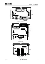
Страница 10: ...Chapter 2 Installation 6 CPC 3811CLD4N 4 00 42 38 46 38 58 16 100 00 CPC 3811CLD4N 2 100 00 19 93 81 50 88 90 60 07 80 00 10 00 77 00 CPC RP3811 1 88 90 5 55 100 00 5 93 66 00 CPC RP3811 2 Unit mm...

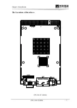
Страница 11: ...Chapter 2 Installation CPC 3811CLD4N 7 The Locations of Interfaces D5 SW1 USB1 LAN1 VGA1 CONN1 JCC1 J2 JTAG1 J1 JP1 CPC 3811CLD4N 1...

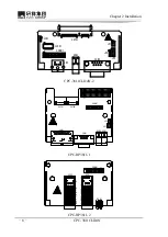
Страница 12: ...hapter 2 Installation 8 CPC 3811CLD4N KM1 CONN1 USB1 COM1 JP2 JP3 JP1 SATA1 LVDS1 JLCD1 CPC 3811CLD4N 2 LAN1 COM1 USB2 USB1 JP1 JP2 CONN1 J1 SATA2 SATA1 CPC RP3811 1 CONN1 SFP2 SFP1 D2 D1 CPC RP3811 2...

Страница 13: ...ar Keep CMOS Setting CMOS is powered by the onboard button battery Clear CMOS will restore original settings factory default The steps are listed as follows a Turn off the computer and unplug the powe...

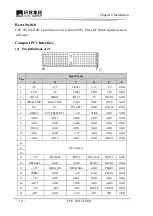
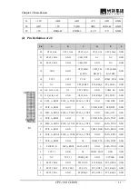
Страница 14: ...I O INTP INTS GND 5 NC NC PCI_RST GND GNT0 GND 6 REQ0 PCI_PRESENT 3 3V CLK0 AD31 GND 7 AD30 AD29 AD28 GND AD27 GND 8 AD26 GND V I O AD25 AD24 GND 9 C BE3 GND AD23 GND AD22 GND 10 AD21 GND 3 3V AD20 AD...

Страница 15: ...CPCI_FAL PCI_REQ5 PCI_GNT5 GND 14 PCIE_A_RXN3 PCIE_A_TXN3 PCIE_A_TXP3 GND USB_DN2 GND 13 PCIE_A_RXP3 GND NC COM2_DTR USB_DP2 GND 12 PCIE_A_RXN2 PCIE_A_TXN2 PCIE_A_TXP2 GND USB_OC23 GND 11 PCIE_A_RXP2...

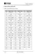
Страница 16: ...ND A17 COM1_CTS A18 COM1_RI A19 COM1_DCD A20 COM1_SOUT A21 KB_DATA A22 KB_CLK A23 VCC12 A24 VCC12 A25 VCC5 B1 LVDS_D0 B2 GND B3 LVDS_D1 B4 GND B5 LVDS_D2 B6 GND B7 LVDS_D3 B8 GND B9 LVDS_CLK B10 USB_O...

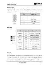
Страница 17: ...og is not operating ON Watchdog is operating Hot swap HS OFF Normal operating status ON Under hot swapping Hard Disk HDD OFF Hard disk is not used ON Hard disk is operating Power PWR OFF Power failure...

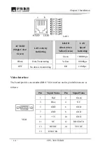
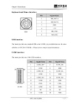
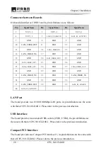
Страница 18: ...g Green 1000Mbps Blink Data Transmitting Yellow 100Mbps OFF No data is transmitting Off 10Mbps Video Interface The board provides one standard DB15 VGA interface and its pin definitions are as follows...

Страница 19: ...ort and OFF is open 2 When using JP3 JP1 shall be set to RS 232 mode 2 JLCD1 LCD Operating Voltage Selection Different LCD screens have different voltages The board provides two kinds of voltages 3 3V...

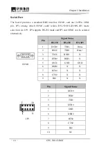
Страница 20: ...realize RS 232 RS 422 RS 485 mode selection via JP1 JP3 supports RS 232 mode and JP3 and COM1 can be selected alternatively COM1 Pin Signal Name RS 232 RS 422 RS 485 1 DCD TXD Data 2 RXD TXD Data 3 TX...

Страница 21: ...andard USB socket USB1 its pin definitions are the same with that of CPC 3811CLD4N 1 Please refer to the previous introduction LVDS Interface The board provides one 18bit LVDS interface LVDS1 Pin Sign...

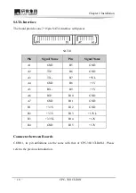
Страница 22: ...Signal Name Pin Signal Name A1 GND B5 GND A2 TX B6 GND A3 TX B7 5VL A4 GND B8 5V A5 RX B9 5V A6 RX B10 GND A7 GND B11 GND B1 3 3V B12 GND B2 3 3V B13 12VL B3 3 3VL B14 12V B4 GND B15 12V Connecter bet...

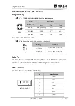
Страница 23: ...short and OFF is open 2 JP2 Operation Mode Selection for LAN Card JP2 Setting Function 1 2 Short Electric Port Operation Default 2 3 Short Optical Port Operation Serial Port The board provides a stan...

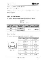
Страница 24: ...IBER_OUT 28 GND 29 GND 30 GND 31 LAN4_FIBER_IN 32 GND 33 LAN4_FIBER_IN 34 GND 35 GND 36 GND 37 LAN4_FIBER_DET 38 GND 39 LAN4_PF_LINKUP 40 LAN4_PF_ACTIVITY LAN Port The board provides two 10 100 1000Mb...

Страница 25: ...cators D1 and D2 D1 D2 ACTLED Single Color Green LAN Activity Indicating LILED Single Color Green LAN Speed Indicating Blink Data Transmitting Green 1000Mbps OFF No data is transmitting Optical LAN Po...

Страница 26: ...Chapter 3 BIOS Setup 22 CPC 3811CLD4N Chapter 3 BIOS Setup Regarding the BIOS features of the motherboard please refer to the AMI BIOS Setup Guide edited by EVOC Company...

Страница 27: ...PnP of BIOS Setup interface to Reserved The following describes WDT program in C language The steps to program WDT are listed as follows Enter WDT programming mode Set WDT operating mode enable WDT di...

Страница 28: ...e needed IRQ number value the variable irq the available range of IRQ numbers are listed at the beginning of this document irq irq 4 outportb pm_base 0x47 0x80 outportb pm_base 0x67 irq 3 Configure WD...

Страница 29: ...stem Timer 060h 064h Standard 101 102 Keyboard Controller 070h 071h Real Time clock NMI 080h 09Fh DMA Page Register 0A0h 0A1h Programmable Interrupt Controller 2 0C0h 0DFh DMA Controller 2 0F0h 0FFh N...

Страница 30: ...diagram below shows parts of the interrupt distribution but it does not show the interrupt source occupied by the PCI devices Level Function IRQ0 System Timer IRQ1 Standard 101 102 Keyboard or Microso...

Страница 31: ......

Страница 32: ...EVOC 2008 1 2 3 10 4 5 6 7 8 9 30...

Страница 33: ...1 1 1 2 2 2 2 2 2 3 3 3 I O 3 4 4 6 CPC 3811CLD4N 1 8 8 JTAG 8 8 Compact PCI 9 11 USB 12 12...

Страница 34: ...12 13 CPC 3811CLD4N 2 14 14 LVDS 14 15 16 USB 16 LVDS 16 SATA 17 17 IO CPC RP3811 1 18 18 18 SATA 18 19 19 USB 19 Compact PCI 19 IO CPC RP3811 2 20 20 20 20 BIOS 21 22 Watchdog 22 I O 24 IRQ 25...

Страница 35: ...ryn L2 cache 3M New SSE4 Intel 3100 Chipset Codename Whitmore Lake 800 FSB 1GB DDR2 ECC REG 3U CompactPCI 4 10 100 1000Mbps 2 SFP PCI PCI 32 32MB VGA LVDS l 20 70 5 95 l 40 C 85 C 5 95 l CPC 3811CLD4N...

Страница 36: ...5 3 l 12V 0 79A 5 3 Intel Core 2 Duo CPU SU9300 800MHz FSB 1 2GHz 3M L2 cache uBGA SFF 956 balls Intel 3100 Chipset 800MHz FSB 1GB 400MHz DDR2 XGI Z9S PCI 32 32MB CRT LVDS CRT 1600x1200 60Hz 2 PCI E...

Страница 37: ...4 CPU 5V IMVP6 MAX8771 GTL 18A Intel 3100 PCI32bit 33 Bus CompactPCI 3U 32bit CompactPCI PICMG2 0 PICMG2 1 1 7 15pin SATA 2 7pin SATA I O l 4 USB2 0 l 2 DB9 1 DB9 RS 232 RS 422 RS485 RS 232 DB9 l 1 PS...

Страница 38: ...4 CPC 3811CLD4N 19 93 86 00 161 50 54 07 74 00 88 90 85 00 10 00 100 00 80 00 CPC 3811CLD4N 1...

Страница 39: ...CPC 3811CLD4N 5 4 00 42 38 46 38 58 16 100 00 CPC 3811CLD4N 2 100 00 19 93 81 50 88 90 60 07 80 00 10 00 77 00 CPC RP3811 1 88 90 5 55 100 00 5 93 66 00 CPC RP3811 2 mm...

Страница 40: ...6 CPC 3811CLD4N D5 SW1 USB1 LAN1 VGA1 CONN1 JCC1 J2 JTAG1 J1 JP1 CPC 3811CLD4N 1...

Страница 41: ...CPC 3811CLD4N 7 KM1 CONN1 USB1 COM1 JP2 JP3 JP1 SATA1 LVDS1 JLCD1 CPC 3811CLD4N 2 LAN1 COM1 USB2 USB1 JP1 JP2 CONN1 J1 SATA2 SATA1 CPC RP3811 1 CONN1 SFP2 SFP1 D2 D1 CPC RP3811 2...

Страница 42: ...8 CPC 3811CLD4N 1 1 2 3 CPC 3811CLD4N 1 1 JCC1 CMOS CMOS CMOS 1 2 JCC1 3 4 BIOS 5 JCC1 1 2 Default 1 2 CMOS BIOS 2 JP1 JP1 1 2 1 2 JTAG JTAG1 1 VCC 2 GND 3 TCK 4 TDO 5 TDI 6 TMS CPC 3811CLD4N 1 SW1...

Страница 43: ...I O AD25 AD24 GND 9 C BE3 GND AD23 GND AD22 GND 10 AD21 GND 3 3V AD20 AD19 GND 11 AD18 AD17 AD16 GND C BE2 GND 12 KEY AREA 13 14 15 3 3V FRAME IRDY BD_SEL TRDY GND 16 DEVSEL GND V I O STOP LOCK GND 17...

Страница 44: ...TXP3 GND USB_DN2 GND 13 PCIE_A_RXP3 GND NC COM2_DTR USB_DP2 GND 12 PCIE_A_RXN2 PCIE_A_TXN2 PCIE_A_TXP2 GND USB_OC23 GND 11 PCIE_A_RXP2 GND NC COM2_RTS SATA_TXP1 GND 10 PCIE_A_RXN1 PCIE_A_TXN1 PCIE_A_T...

Страница 45: ...A A22 KB_CLK A23 VCC12 A24 VCC12 A25 VCC5 B1 LVDS_D0 B2 GND B3 LVDS_D1 B4 GND B5 LVDS_D2 B6 GND B7 LVDS_D3 B8 GND B9 LVDS_CLK B10 USB_OC1 B11 USB_DN1 B12 GND B13 SATA_RXP0 B14 GND B15 SATA_TXP0 B16 LV...

Страница 46: ...12 CPC 3811CLD4N USB USB USB1 1 5V 2 USB_Data 3 USB_Data 4 GND D5 WDT OFF ON HS OFF ON HDD OFF ON PWR OFF ON CPC 3811CLD4N 1 2 10 100 1000Mbps LILED ACTLED LAN LED...

Страница 47: ...CPC 3811CLD4N 13 LAN1 ACTLED LILED 1000Mbps 100Mbps 10Mbps DB15 VGA VGA1 1 Red 2 Green 3 Blue 4 NC 5 GND 6 GND 7 GND 8 GND 9 5V 10 GND 11 NC 12 DDCDATA 13 HSYNC 14 VSYNC 15 DDCCLK...

Страница 48: ...JP1 RS 232 RS 422 RS 485 JP1 1 2 3 4 5 6 RS 232 ON Default OFF OFF RS 422 OFF OFF ON RS 485 OFF ON OFF 1 ON OFF 2 JP3 JP1 RS 232 2 JLCD1 LCD LCD 3 3V 5V LCD LCD LCD JLCD1 1 2 3 3V Default 2 3 5V LVDS...

Страница 49: ...JP1 RS 232 RS 422 RS 485 JP3 RS 232 JP3 COM1 COM1 RS 232 RS 422 RS 485 1 DCD TXD Data 2 RXD TXD Data 3 TXD RXD X 4 DTR RXD X 5 GND GND GND 6 DSR X X 7 RTS X X 8 CTS X X 9 RI X X JP3 1 DCD 2 RXD 3 TXD...

Страница 50: ...DATA 3 GND 4 5V 5 KB_CLK 6 MS_CLK USB USB USB1 CPC 3811CLD4N 1 LVDS 18bit LVDS LVDS1 1 LVDS_D0 2 LVDS_D0 3 GND 4 GND 5 LVDS_D1 6 LVDS_D1 7 GND 8 GND 9 LVDS_D2 10 LVDS_D2 11 GND 12 GND 13 CLK 14 CLK 15...

Страница 51: ...D4N 17 SATA 7 15pin SATA SATA1 A1 GND B5 GND A2 TX B6 GND A3 TX B7 5VL A4 GND B8 5V A5 RX B9 5V A6 RX B10 GND A7 GND B11 GND B1 3 3V B12 GND B2 3 3V B13 12VL B3 3 3VL B14 12V B4 GND B15 12V CONN1 CPC...

Страница 52: ...1 JP1 RS 232 RS 422 RS 485 JP1 1 2 3 4 5 6 RS 232 ON Default OFF OFF RS 422 OFF OFF ON RS 485 OFF ON OFF ON OFF 2 JP2 JP2 1 2 Default 2 3 DB9 COM1 CPC 3811CLD4N 2 COM1 SATA 7Pin SATA SATA1 SATA2 1 GN...

Страница 53: ...ER_IN 17 GND 18 GND 19 GND 20 LAN3_FIBER_OUT 21 GND 22 LAN3_FIBER_OUT 23 GND 24 GND 25 LAN4_FIBER_OUT 26 GND 27 LAN4_FIBER_OUT 28 GND 29 GND 30 GND 31 LAN4_FIBER_IN 32 GND 33 LAN4_FIBER_IN 34 GND 35 G...

Страница 54: ...00Mbps D1 D2 D1 D2 ACTLED LILED 1000Mbps 1000Mbps SFP1 SFP2 SFP1 SFP2 1 T_GND 11 R_GND 2 TX_FAULT 12 RX 3 TX_DISABLE 13 RX 4 MOD_DEF 2 14 R_GND 5 MOD_DEF 1 15 VCC_RX 6 MOD_DEF 0 16 VCC_TX 7 RATE SELEC...

Страница 55: ...BIOS CPC 3811CLD4N 21 BIOS BIOS AMI BIOS...

Страница 56: ...efine DATA_PORT 0x2F unsigned int tmp_reg unsigned int pm_base outportb INDEX_PORT 0x55 outportb INDEX_PORT 0x07 outportb DATA_PORT 0x0A outportb INDEX_PORT 0x30 outportb DATA_PORT 0x01 outportb INDEX...

Страница 57: ...ned int irq irq IRQ_NO IRQ_NO irq irq irq 4 outportb pm_base 0x47 0x80 outportb pm_base 0x67 irq 3 WDT a outportb pm_base 0x65 0x00 b outportb pm_base 0x65 0x80 4 WDT a WDT outportb pm_base 0x66 TIME_...

Страница 58: ...21h 1 040h 043h 060h 064h 101 102 070h 071h NMI 080h 09Fh DMA 0A0h 0A1h 2 0C0h 0DFh DMA 2 0F0h 0FFh 170h 177h IDE 1F0h 1F7h IDE 274h 277h PnP 279h A79h PnP 2F8h 2FFh 2 COM2 376h IDE dual FIFO 3B0h 3DF...

Страница 59: ...CPC 3811CLD4N 25 IRQ 15 ISA ISA BIOS PCI BIOS CPU PCI IRQ0 IRQ1 101 102 Microsoft IRQ2 IRQ3 2 IRQ4 1 IRQ5 IRQ6 IRQ7 IRQ8 CMOS IRQ9 Int 0Ah IRQ10 IRQ11 IRQ12 IRQ13 IRQ14 IDE IRQ15 IDE http www evoc com...

Отзывы: