Epson Q41856470000100 Скачать руководство пользователя страница 13

RTC - 8564 JE/NB 


Page - 10 

MQ - 322 - 04 


8.3.7. I

2

C-BUS protocol 


The following section describes the communications procedure where the master is CPU and the slave is the 
RTC-8564. 


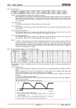
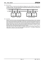
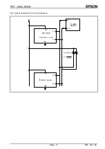
(1) Procedure for write at specified address 


The RTC-8564 has an auto increment function of address. After the initial address is set, if only data continues 
to be sent, the receiving address on the 8564 is incremented by 1 byte. The procedure as follows: 


(1) The CPU sends out a start condition. 
(2) The CPU sends out the slave address of the 8564 and the R/W bit, in write mode. 
(3) Confirm acknowledge from the 8564. 
(4) The CPU sends out the write address to the 8564. 
(5) Confirm acknowledge from the 8564. 
(6) The CPU sends out the data for write to the address specified in step (4). 
(7) Confirm acknowledge from the 8564. 
(8) If necessary repeat steps (6) and (7). The address will be automatically incremented internally on the 8564. 
(9) The CPU sends out the stop condition. 


(1) 

R/W 

(3) 

Address 

(4) 

(5) 


Data 

(8) 

(9) 

Acknowledge from the 8564 

Data 

(6) 

(7) 

(2) 

Slave address 


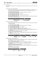
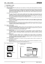
(2) Procedure for read at specified address 


According to the write mode, after the address to read is written, the read mode is set and the actual data read. 
The procedure as follows: 


(1)   The CPU sends out a start condition. 
(2)   The CPU sends out the slave address of the 8564 and the R/W bit, in write mode. 
(3)   Confirm acknowledge from the 8564. 
(4)   The CPU sends out the address read out from the 8564. 
(5)   Confirm acknowledge from the 8564. 
(6)   The CPU sends out the start condition (stop condition is not sent.) 
(7)   The CPU sends out the slave address of the 8564 and the R/W bit, in read mode. 
(8)   Confirm acknowledge from the 8564.(From here on, the CPU acts as a receiver and the 8564 as a 

transmitter.) 

(9)   Data at the address specified in step (4) is sent out from the 8564. 
(10) The CPU sends out acknowledge to the 8564. 
(11) If necessary repeat steps (9) and (10). The read address will be automatically incremented internally on 

the 8564. 

(12) The CPU sends out the stop condition. 


(1) 

R/W 

(3) 

Address 

(4) 

(6) 

(5) 

R/W 

(8) 

Data 

(9) 


(10) 


Data 

(11) 

(13) 

(12) 

Acknowledge from the 8564 

Acknowledge from the CPU 

(2) 

Slave address 

(7) 

Slave address 


(3) Read procedure without specified address 


Immediately after the read mode is set up, data can be read. In this case, the address is the address when the 
previous access ended, plus 1. The procedure is as follows: 


(1) The CPU sends out a start condition. 
(2) The CPU sends out the slave address of the 8564 and the R/W bit, in read mode. 
(3) Confirm acknowledge from the 8564.(From here on, the CPU acts as a receiver and the 8564 as a 

transmitter.) 

(4) Data at the last address in the previous access plus 1 is sent out from the 8564. 
(5) The CPU sends out acknowledge to the 8564. 
(6) If necessary repeat steps (4) and (5). The read address will be automatically incremented internally on the 

8564. 

(7) The CPU sends out acknowledge of "1". 
(8) The CPU sends out the stop condition. 


(1) 

R/W 

(3) 

Data 

(4) 

(5) 


(7) 

Data 

(6) 

(8) 

Acknowledge from the CPU 

Acknowledge from the 8564 

(2) 

Slave address 


Содержание Q41856470000100

Страница 1: ...MQ322 04 Application Manual Real Time Clock Module RTC 8564JE NB Model Product Number RTC 8564JE Q41856470000100 RTC 8564NB Q41856490000200 ...

Страница 2: ...intellectual property rights is granted by implication or otherwise and there is no representation or warranty that anything made in accordance with this material will be free from any patent or copyright infringement of a third party This material of portions thereof may contain technology or the subject relating to strategic products under the control of the Foreign Exchange and Foreign Trade La...

Страница 3: ...8 2 2 Control register 2 6 8 2 3 Clock and calendar registers and VL bit and century bit 6 8 2 4 Alarm registers 7 8 2 5 CLKOUT frequency selection and timer registers 7 8 3 Access procedure 8 8 3 1 Characteristic of the I 2 C BUS 8 8 3 2 Bit transfer 8 8 3 3 Start condition and stop condition 8 8 3 4 Slave address 8 8 3 5 System structure 9 8 3 6 Acknowledge 9 8 3 7 I 2 C BUS protocol 10 8 4 Typi...

Страница 4: ...is module is a serial interface real time clock that has a built in crystal oscillator The module offers many functions such as calendar clock alarm and timer All of them can be controlled with a two 2 lines interface Also the regular frequency output can be selected from programs Because this module has multiple features packaged in the same surface it is ideally suited for applications such as m...

Страница 5: ...ram The pin is an C MOS terminal When initial power is supplied power supply starting from 0 V the power on reset function causes 32 768 kHz to be output When output stops the CLKOUT pin goes to LOW Control of CLKOE pin is necessaryto control this function justly SCL 6 6 Input For input of the serial clock SDA 7 5 Bi Directional This pin synchronizes with a serial clock and input output address da...

Страница 6: ...characteristics Top Ta 10 to 70 C VDD 3 0 V Reference at 25 C 10 120 10 6 Oscillation startup up time tSTA Ta 25 C VDD 1 8 V 3 Max s Aging fa Ta 25 C VDD 3 0 V first year 5 Max 10 6 year 1 Equivalent to 1 minute of monthly deviation excluding offset 7 Electrical characteristics 7 1 DC electrical characteristics If not specifically indicated GND 0 V VDD 1 8 V to 5 5 V Ta 40 C to 85 C Parameter Symb...

Страница 7: ...SU STO 0 6 µs Bus free time between a STOP and START condition tBUF 1 3 µs SCL L time tLOW 1 3 µs SCL H time tHIGH 0 6 µs SCL and SDA rise time tr 0 3 µs SCL and SDA fall time tf 0 3 µs Tolerance spike time on bus tSP 50 ns Timing chart tHD DAT tSU DAT tHD STA tLOW tHIGH 1 fSCL tr tf tSU STA SDA SCL START CONDITION S BIT 7 MSB A7 BIT 6 A6 ACK A Protocol tBUF tSU STO STOP CONDITION P START CONDITIO...

Страница 8: ... mode is a special operation mode that is used by EPSON for testing devices Be sure not to set it to 1 If it is set to the test mode all operations of the device will not be guaranteed Therefore be careful when access to address 00 3 Be sure to set bit 0 of address 00 01 Control1 2 to zero 4 All count data at address 02 through 05 and 08 through 0B is in the BCD format 5 Write to bit is not possib...

Страница 9: ... timer are both prohibited The INT pin will not become LOW active If all hardware interrupts cannot be used due to system constraints after the above setup be sure to use the software to monitor the interrupt flags for AF and TF 8 2 3 Clock and calendar registers and VL bit and century bit Address Function bit 7 bit 6 bit 5 bit 4 bit 3 bit 2 bit 1 bit 0 02 Seconds VL 40 20 10 8 4 2 1 03 Minutes 40...

Страница 10: ...et When all of the bits are set to AE no alarm will occur Additional information on the alarm function Even when the alarm is turned on for a long time this device clears the flag when the alarm occurs once and so no more further alarm will occur under the same condition This means in the same day when the alarm condition is met once the alarm flag is cleared and the alarm becomes unmatched the al...

Страница 11: ...rt condition After that actual data transfer is executed When SCL is at HIGH and when SDA changes from LOW to HIGH this is defined as a stop condition SDA SCL S P Start condition Stop condition 8 3 4 Slave address The I 2 C BUS devices do not have any chip select pins with the usual logic devices All I 2 C BUS devices have a fixed unique device number for each device built into them The chip selec...

Страница 12: ...as received the data Because the acknowledge bit is LOW active the transmitter sets the SDA line to HIGH and sends out a clock pulse for the acknowledge bit If the receiver can correctly receive the 8 bit data from the transmitter it will set the SDA line to LOW when the clock for the last bit is finished Because the I 2 C BUS lines are pulled up the SDA line of transmitter also turns to LOW At th...

Страница 13: ...d out from the 8564 5 Confirm acknowledge from the 8564 6 The CPU sends out the start condition stop condition is not sent 7 The CPU sends out the slave address of the 8564 and the R W bit in read mode 8 Confirm acknowledge from the 8564 From here on the CPU acts as a receiver and the 8564 as a transmitter 9 Data at the address specified in step 4 is sent out from the 8564 10 The CPU sends out ack...

Страница 14: ... 8564 JE NB Page 11 MQ 322 04 8 4 Typical connection to micro computers device SCL SDA GND VDD Master VDD SCL SDA tr R CBUS Pull up Registor RTC 8564 SCL SDA GND VDD SLAVE ADRS 1010001 I C BUS 2 I C BUS 2 ...

Страница 15: ...Soldering pattern 1 3 0 1 0 125 0 1 Unit mm 6 3 Max 5 0 0 2 4 8 0 5 0 2 1 22 14 11 14 0 3 11 1 22 0 8 P 0 5 10 5 0 1 4 0 5 5 25 0 25 0 7 0 75 0 25 0 8 0 7 4 0 0 7 0 7 1 11 22 14 1 The cylinder of the crystal oscillator can be seen in this area back and front but it has no affect on the performance of the device 2 In this area At a parts side of electronic base you must not do layout any signal lin...

Страница 16: ...ge 3 How to find the date difference Date Difference f f 86400 Sec For example f f 11 574 10 6 is an error of approximately 1 second day 1 Example of frequency and temperature characteristics 150 100 50 0 50 0 50 100 Temperature C Frequency f T 10 6 θT 25 C Typ α 0 035 10 6 Typ 2 Example of frequency and voltage characteristics 3 2 Frequency f v 10 6 3 0 3 4 5 Condition 3 V as reference Ta 25 C Su...

Страница 17: ... level and malfunctions due to noise Therefore pull up or pull down resistors should be provided for all unused input pins 11 2 Notes on packaging 1 Soldering temperature conditions If the temperature within the package exceeds 260 the characteristics of the crystal oscillator will be degraded and it may be damaged Therefore always check the mounting temperature before mounting this device Also ch...

Страница 18: ... 0 1344 381700 Fax 44 0 1344 381701 FRENCH Branch Office LP 915 Les Conquérants 1 Avenue de l Atlantique Z A de Courtaboeuf 2 91976 Les Ulis Cedex France Phone 33 0 1 64862350 Fax 33 0 1 64862355 ASIA EPSON CHINA CO LTD 23F Beijing Silver Tower 2 North RD DongSangHuan ChaoYang District Beijing China Phone 86 10 6410 6655 Fax 86 10 6410 7319 http www epson com cn 4F Bldg 27 No 69 Gui Qing Road Cao ...

Отзывы: