background image

3  FUNCTION OPTION GENERATOR FOG6011

E0C6011 DEVELOPMENT TOOL MANUAL

EPSON

11

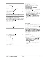
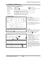
Select the output specification for the R01 terminal.
Either complementary output or Pch open drain
output may be selected.
The circuit configuration is the same as that of the
output port R00 (Figure 3.3.2).

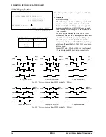
6 R01 specification

*** OPTION  NO.6 ***

--- << R01 SPECIFICATION >> ---

 R01 OUTPUT SPECIFICATION  1. COMPLEMENTARY
                           2. PCH-OPENDRAIN

PLEASE SELECT NO.(1) ? 1

 R01 OUTPUT SPECIFICATION  1. COMPLEMENTARY SELECTED

7 R02 specification

*** OPTION  NO.7 ***

--- << R02 SPECIFICATION >> ---

 R02 OUTPUT SPECIFICATION  1. COMPLEMENTARY
                           2. PCH-OPENDRAIN

PLEASE SELECT NO.(1) ? 1

 R02 OUTPUT TYPE           1. DC
                           2. FOSC/2
                           3. FOSC/4
                           4. FOSC/8
                           5. FOSC/16
                           6. FOSC/32
                           7. FOSC/64
                           8. FOSC/128
                           9. FOSC/256

PLEASE SELECT NO.(1) ? 1

 R02 OUTPUT SPECIFICATION  1. COMPLEMENTARY SELECTED
 R02 OUTPUT TYPE           1. DC SELECTED

Select the output specification and the output type
for the R02 terminal.

Output specification
Either complementary output or Pch open drain
output may be selected.
The circuit configuration is the same as that of the
output port R00 (Figure 3.3.2).

Output type
Either DC output or FOUT output may be
selected.
When DC output is selected, R02 becomes a
regular output port.
When the R02 register is set to "1", the R02
terminal output goes high (V

DD

), and goes low

(V

SS

) when set to "0".

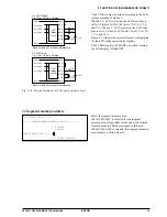
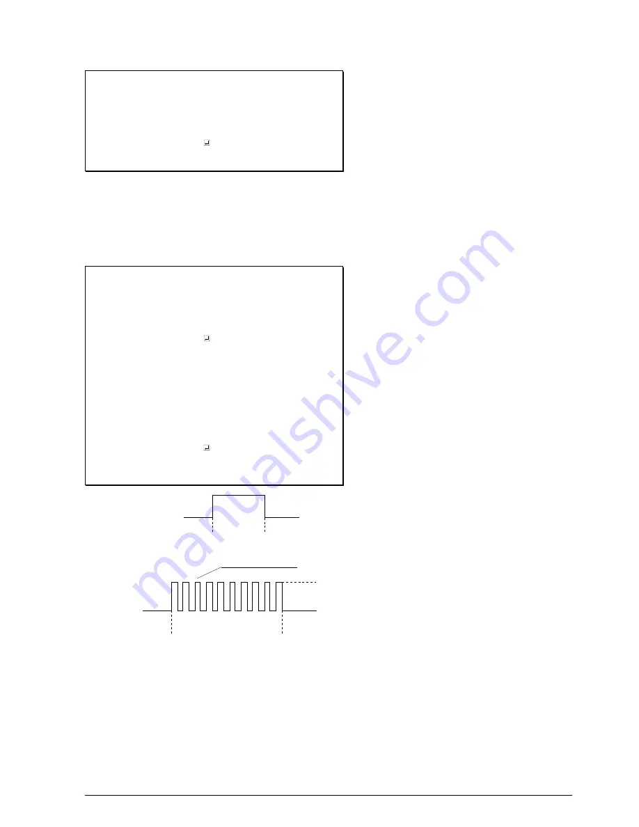
The output waveform is shown in Figure 3.3.3.

When FOUT is selected, a clock with a set
frequency can be output from the R02 terminal.
When the FOUT bit (R02 register) is set to "1",
50% duty and V

DD

–V

SS

 amplitude square wave is

generated at the specified frequency. When set to
"0", the FOUT terminal goes low (V

SS

). A FOUT

frequency may be selected from among 8 types,
ranging from f

OSC

/256 to f

OSC

/2.

The FOUT output is normally utilized to provide
clock to other devices but since hazard occurs at
the square wave breaks, great caution must be
observed when using it.
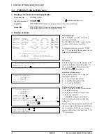
The output waveform is shown in Figure 3.3.4.

Fig. 3.3.3  Output waveform at R02 DC output selection

V

DD

V

SS

0

1

0

R02 register

R02 output

Fig. 3.3.4  Output waveform at R02 FOUT output selection

R02 output

R02 register

0

1

0

Specified frequency

V

DD

V

SS

Содержание E0C6011

Страница 1: ...MF1224 01 CMOS 4 BIT SINGLE CHIP MICROCOMPUTER E0C6011 DEVELOPMENT TOOL MANUAL ...

Страница 2: ...ty that anything made in accordance with this material will be free from any patent or copyright infringement of a third party This material or portions thereof may contain technology or the subject relating to strategic products under the control of the Foreign Exchange and Foreign Trade Control Law of Japan and may require an export license from the Ministry of International Trade and Industry o...

Страница 3: ... CONTENTS 1 COMPOSITION OF DEVELOPMENT SUPPORT TOOL _____________ 1 1 1 Configuration of DEV6011 1 1 2 Developmental Environment 1 1 3 Development Flow 2 1 4 Production of Execution Disk 3 2 CROSS ASSEMBLER ASM6011 __________________________________ 4 2 1 ASM6011 Outline 4 2 2 E0C6011 Restrictions 4 2 3 ASM6011 Quick Reference 5 3 FUNCTION OPTION GENERATOR FOG6011 ______________________ 7 3 1 FOG6...

Страница 4: ...__________________ 32 6 1 MDC6011 Outline 32 6 2 MDC6011 Quick Reference 32 APPENDIX A E0C6011 INSTRUCTION SET ________________________ 35 B E0C6011 RAM MAP ________________________________ 39 C E0C6011 I O MEMORY MAP _________________________ 40 D TROUBLESHOOTING ______________________________ 41 ...

Страница 5: ...n program 1 2 Developmental Environment The software product of the development support tool DEV6011 operates on the following host systems IBM PC AT at least PC DOS Ver 2 0 NEC PC 9801 Series at least MS DOS Ver 3 1 When developing the E0C6011 the above mentioned host computer editor P ROM writer printer etc must be prepared by the user in addition to the development tool which is normally suppor...

Страница 6: ... Generator FOG6011 execution Segment Option Generator SOG6011 execution Determination of software specifications Cross Assembler ASM6011 execution Source file generation by using editor Function option list Segment option list C011XXX DAT Program source file Coding sheet Flow chart generation and coding Source file generation by using editor C011XXX SEG Segment option source file C011XXXL HEX Obje...

Страница 7: ...ing the COPY command Example Copying into a floppy disk Insert the original disk into the A drive and the formatted disk to be copied into B drive then execute the DISKCOPY command A DISKCOPY A B Copying into a hard disk C drive Make a subdirectory DEV6011 then insert the original disk into the A drive and execute the COPY command C MD DEV6011 C CD DEV6011 C DEV6011 COPY A Example Setting of FILES...

Страница 8: ...e E0C62 Family Development Tool Reference Manual for details ROM area The capacity of the E0C6011 ROM is 1 536 steps 0000H to 05FFH Therefore the specification range of the memory setting pseudo instructions and PSET instruction is restricted Memory configuration Bank Only bank 0 Page 6 pages 0 to 5H each 256 steps Significant specification range ORG pseudo instruction 0000H to 05FFH PAGE pseudo i...

Страница 9: ...PPP SSSSSSS OOOOOOOO NNN NN C COPYRIGHT 1999 SEIKO EPSON CORP SOURCE FILE NAME IS C011XXX DAT THIS SOFTWARE MAKES NEXT FILES C011XXXH HEX HIGH BYTE OBJECT FILE C011XXXL HEX LOW BYTE OBJECT FILE C011XXX PRN ASSEMBLY LIST FILE DO YOU NEED AUTO PAGE SET Y N Y 1 DO YOU NEED CROSS REFERENCE TABLE Y N Y 2 When ASM6011 is started the start up message is displayed At 1 select whether or not the auto page ...

Страница 10: ...tered The label or symbol of the operand has not been defined The label field has been omitted A syntax error was encountered in the operand or the operand could not be evaluated Error message Syntax Error Undefined Error Missing Label Operand Error Phase Error Range Error Warning Explanation The same label or symbol was defined more than once The source file name was longer than 8 characters The ...

Страница 11: ...d by a general purpose computer The HEX file for the evaluation board EVA6011 hardware option ROM is simultaneously generated with the data file Fig 3 1 1 FOG6011 execution flow 3 2 E0C6011 Option List Multiple specifications are available in each option item as indicated in the Option List Using 3 3 Option Specifications and Selection Message as reference select the specifications that meet the t...

Страница 12: ...n P02 1 Complementary 2 Pch OpenDrain P03 1 Complementary 2 Pch OpenDrain P10 1 Complementary 2 Pch OpenDrain P11 1 Complementary 2 Pch OpenDrain P12 1 Complementary 2 Pch OpenDrain P13 1 Complementary 2 Pch OpenDrain 10 I O PORT PULL DOWN RESISTOR P00 1 With Resistor 2 Gate Direct P01 1 With Resistor 2 Gate Direct P02 1 With Resistor 2 Gate Direct P03 1 With Resistor 2 Gate Direct P10 1 With Resi...

Страница 13: ... a CR oscillation circuit with resistor and capacitor built in Four frequencies are available 3 3 Option Specifications and Selection Message Screen that can be selected as function options set on the E0C6011 are shown below and their specifications are also described OPTION NO 3 INTERRUPT NOISE REJECTOR K00 K03 1 USE 2 NOT USE PLEASE SELECT NO 1 1 1 USE SELECTED Select whether noise rejector will...

Страница 14: ...03 2 GATE DIRECT SELECTED Select whether input ports K00 K03 will each be supplemented with pull down resistors or not When Gate Direct is selected see to it that entry floating state does not occur Select With Resistor for unused ports Moreover the input port status is changed from high level VDD to low VSS with pull down resistors a delay of approximately 1 msec in waveform rise time will occur ...

Страница 15: ...output may be selected The circuit configuration is the same as that of the output port R00 Figure 3 3 2 Output type Either DC output or FOUT output may be selected When DC output is selected R02 becomes a regular output port When the R02 register is set to 1 the R02 terminal output goes high VDD and goes low VSS when set to 0 The output waveform is shown in Figure 3 3 3 When FOUT is selected a cl...

Страница 16: ...r output is selected inverted wave form of R00 buzzer output is generated from the R03 terminal When BZ OUTPUT R03 is selected the R03 outputs the buzzer inverted signal when 1 is written to the R03 register When BZ OUTPUT R00 is selected the R03 buzzer output can be controlled by the R00 register as well as the R00 buzzer output The buzzer output for R03 may not be selected when the output type o...

Страница 17: ...t line and the built in pull down resistor load is greater than the read out time When the input data is being read the time that the input line is pulled down is equivalent to 0 5 cycles of the CPU system clock Hence the electric potential of the terminals must settle within 0 5 cycles If this condition cannot be met some measure must be devised such as arranging a pull down resistor externally o...

Страница 18: ...ND BIAS 1 1 4 DUTY 1 2 BIAS 2 1 3 DUTY 1 2 BIAS 3 1 2 DUTY 1 2 BIAS PLEASE SELECT NO 1 1 1 1 4 DUTY 1 2 BIAS SELECTE Select the specification drive duty for the LCD drive circuit Drive duty Select a drive duty When 1 2 duty is selected up to 76 segments of LCD panel can be driven with 2 COM terminals and 38 SEG terminals When 1 3 duty is selected up to 114 segments can be driven with 3 COM termina...

Страница 19: ...ent memory area When 40H 6FH is selected for the segment memory area it is possible to read and write from to this area because a RAM is assigned to this area When C0H EFH is selected this segment memory area becomes a write only area OPTION NO 12 SEGMENT MEMORY ADDRESS SELECT 1 40H 6FH 2 C0H EFH PLEASE SELECT NO 1 2 2 C0H EFH SELECTED VDD VL1 VL2 VL3 CA CB VSS 1 5 V C2 C3 C1 0 1µF 0 1µF 0 1µF VDD...

Страница 20: ... C keys together the sequence returns to the DOS command level Setting new function options Select 1 on the operation selection menu 1 Enter the file name 2 Enter the customer s company name 3 Enter any comment Within 50 characters x 10 lines Next start function option setting from option No 1 In case a function option document file with the same name as the file name specified in the current driv...

Страница 21: ... FILE NAME In step 2 if the function option document file is not in the current drive the following message is displayed prompting entry of other file name END OF OPTION SETTING DO YOU MAKE HEX FILE Y N Y 1 OPTION EPROM SELECT MENU 1 27C64 2 27C128 3 27C256 4 27C512 PLEASE SELECT NO 2 2 2 27C128 SELECTED MAKING FILE S IS COMPLETED OPERATION SELECT MENU 1 INPUT NEW FILE 2 EDIT FILE 3 RETURN TO DOS ...

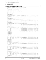
Страница 22: ...01 01 OPTION NO 4 INPUT PORT PULL DOWN RESISTOR K00 WITH RESISTOR SELECTED K01 WITH RESISTOR SELECTED K02 WITH RESISTOR SELECTED K03 WITH RESISTOR SELECTED OPT0401 01 OPT0402 01 OPT0403 01 OPT0404 01 OPTION NO 5 R00 SPECIFICATION R00 OUTPUT SPECIFICATION COMPLEMENTARY SELECTED R00 OUTPUT TYPE DC SELECTED OPT0501 01 OPT0502 01 OPTION NO 6 R01 SPECIFICATION R01 OUTPUT SPECIFICATION COMPLEMENTARY SEL...

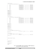
Страница 23: ...RT PULL DOWN RESISTOR P00 WITH RESISTOR SELECTED P01 WITH RESISTOR SELECTED P02 WITH RESISTOR SELECTED P03 WITH RESISTOR SELECTED P10 WITH RESISTOR SELECTED P11 WITH RESISTOR SELECTED P12 WITH RESISTOR SELECTED P13 WITH RESISTOR SELECTED OPT1001 01 OPT1002 01 OPT1003 01 OPT1004 01 OPT1005 01 OPT1006 01 OPT1007 01 OPT1008 01 OPTION NO 11 LCD COMMON DUTY AND BIAS 1 4 DUTY 1 2 BIAS SELECTED OPT1101 0...

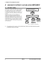
Страница 24: ... file used to generate mask patterns From the data file created with SOG6011 the E0C6011 mask pattern is auto matically generated by a general purpose computer The HEX file for the evaluation board EVA6011 segment option ROM is simultaneously generated with the data file Fig 4 1 1 SOG6011 execution flow A EDLIN C011XXX SEG Segment source file generation A SOG6011 Execute the segment option generat...

Страница 25: ... SEG31 SEG32 SEG33 SEG34 SEG35 SEG36 SEG37 L H D L H D L H D L H D SEG output DC output SEG output DC output SEG output DC output SEG output DC output SEG output DC output SEG output DC output SEG output DC output SEG output DC output SEG output DC output SEG output DC output SEG output DC output SEG output DC output SEG output DC output SEG output DC output SEG output DC output SEG output DC outp...

Страница 26: ... not possible The allocated segment displays when the bit for this segment memory is set to 1 and goes out when bit is set to 0 Segment allocation is set to H for high address 4 6 or C E to L for low address 0 F and to D for data bit 0 3 and are recorded in their respective column in the option list For segment ports that will not be used write hyphen in the H L and D columns of COM0 COM3 Examples...

Страница 27: ...S C0110A0 C0110B0 C0110C0 1 PLEASE INPUT SEGMENT OPTION FILE NAME C0110A0 2 PLEASE INPUT USER S NAME SEIKO EPSON CORP 3 PLEASE INPUT ANY COMMENT ONE LINE IS 50 CHR FUJIMI PLANT 4 281 FUJIMI SUWA GUN NAGANO KEN 399 0293 JAPAN TEL 0266 61 1211 FAX 0266 61 1273 PLEASE INPUT SEGMENT OPTION SOURCE FILE NAME C0110N0 SEGMENT OPTION SOURCE FILE IS NOT FOUND 7 H option not use PLEASE INPUT SEGMENT OPTION D...

Страница 28: ...ed while setting segment options MAKING FILE IS COMPLETED will be displayed and the SOG6011 program will be terminated END OF OPTION SETTING DO YOU MAKE HEX FILE Y N Y 1 OPTION EPROM SELECT MENU 1 27C64 2 27C128 3 27C256 4 27C512 PLEASE SELECT NO 2 2 2 27C128 SELECTED MAKING FILE IS COMPLETED Error messages S N R D Out Port Set Error The data was written in an invalid format The segment number out...

Страница 29: ...1 C92 C93 S 10 CA0 CA1 CA2 CA3 S 11 CB0 CB1 CB2 CB3 S 12 CC0 CC1 CC2 CC3 S 13 CD0 CD1 CD2 CD3 S 14 CE0 CE1 CE2 CE3 S 15 CF0 CF1 CF2 CF3 S 16 D00 D01 D02 D03 S 17 D10 D11 D12 D13 S 18 D20 D21 D22 D23 S 19 D30 D31 D32 D33 S 20 D40 D41 D42 D43 S 21 D50 D51 D52 D53 S 22 D60 D61 D62 D63 S 23 D70 D71 D72 D73 S 24 D80 D81 D82 D83 S 25 D90 D91 D92 D93 S 26 DA0 DA1 DA2 DA3 S 27 DB0 DB1 DB2 DB3 S 28 DC0 DC1...

Страница 30: ...C93 S 10 CA0 CA1 CA2 CA3 S 11 CB0 CB1 CB2 CB3 S 12 CC0 CC1 CC2 CC3 S 13 CD0 CD1 CD2 CD3 S 14 CE0 CE1 CE2 CE3 S 15 CF0 CF1 CF2 CF3 S 16 D00 D01 D02 D03 S 17 D10 D11 D12 D13 S 18 D20 D21 D22 D23 S 19 D30 D31 D32 D33 S 20 D40 D41 D42 D43 S 21 D50 D51 D52 D53 S 22 D60 D61 D62 D63 S 23 D70 D71 D72 D73 S 24 D80 D81 D82 D83 S 25 D90 D91 D92 D93 S 26 DA0 DA1 DA2 DA3 S 27 DB0 DB1 DB2 DB3 S 28 DC0 DC1 DC2 D...

Страница 31: ...ference Manual for details 5 2 ICS6011 Restrictions Take the following precautions when using the ICS6011 ROM Area The ROM area is limited to a maximum address of 5FFH Assigning data above the 5FFH address causes an error RAM Area The RAM area is limited to a maximum address of 0FFH Assigning data above the 0FFH address causes an error Furthermore as the following addresses are in the unused area ...

Страница 32: ... memory It is HEX file output by the function option generator and has intel HEX format 2 Load segment option HEX file in the EVA6011 segment option data memory It is HEX file output by the segment option generator and has intel HEX format Function Examples OPTLD 1 C011XXX C011XXXF HEX file is loaded in the function option data memory OPTLD 2 C011XXX C011XXXS HEX file is loaded in the segment opti...

Страница 33: ...When ICS6011 is started the start up message is displayed and a self test is automatically performed ICS6011 commands are awaited when the program is properly loaded and the mark is displayed Debugging can be done by entering command after the mark The ICS6011 program is terminated by entering the Q Quit command Note Confirm that the cables con nected properly then operate the ICS6011 Error messag...

Страница 34: ... step instruction from a address Displays only the final step of T a n Sets Break at program address a Breakpoint is canceled Break condition is set for data RAM Breakpoint is canceled Break condition is set for EVA6011 CPU internal registers Breakpoint is canceled Combined break conditions set for program data RAM address and registers Cancel combined break conditions for program data ROM address...

Страница 35: ... history acquisition program area Retrieves and indicates the history information which executed a program address a Retrieves and indicates the history information which wrote or read the data area address a Save contents of memory to program file Save contents of memory to data file Load ICE62R ICE6200 set condition from file Save ICE62R ICE6200 set condition to file Load function option data fr...

Страница 36: ... C011XXXL HEX Object file low order C011XXXH HEX Object file high order C011XXXF DOC Function option document file C011XXXS DOC Segment option document file C6011XXX PAn Packed file When unpacking Output file C6011XXX PAn Packed file When packing C011XXXL PAn Object file low order C011XXXH PAn Object file high order C011XXXF PAn Function option document file C011XXXS PAn Segment option document fi...

Страница 37: ...t up message When MDC6011 is started the start up message and operation menu are displayed Here the user is prompted to select operation options OPERATION MENU 1 PACK 2 UNPACK PLEASE SELECT NO 1 1 C011XXXH HEX C011XXXL HEX C6011XXX PAn PACK FILE C011XXXF DOC C011XXXS DOC PLEASE INPUT PACK FILE NAME C6011XXX PAn C60110A0 PA0 2 C0110A0H HEX C0110A0L HEX C60110A0 PA0 C0110A0F DOC C0110A0S DOC OPERATI...

Страница 38: ...TION DATA ERROR START MARK 2 OPTION DATA ERROR OPTION NUMBER 3 OPTION DATA ERROR SELECT NUMBER 4 OPTION DATA ERROR END MARK The start mark is not OPTION during unpacking The option number is not correct The option selection number is not correct The end mark is not END packing or END unpacking Error Message Explanation 1 SEGMENT DATA ERROR START MARK 2 SEGMENT DATA ERROR DATA 3 SEGMENT DATA ERROR ...

Страница 39: ... y0 r0 r0 r0 r0 r0 r0 r0 r0 i0 i0 i0 i0 p s C s NC s Z s NZ s s s X Y X x Y y XH r XL r YH r YL r r XH r XL r YH r YL XH i XL i YH i YL i PSET JP JPBA CALL CALZ RET RETS RETD NOP5 NOP7 HALT SLP INC LD ADC I D Z C 5 5 5 5 5 5 5 7 7 7 12 12 5 7 5 5 5 5 5 5 5 5 5 5 5 5 5 5 7 7 7 7 NBP p4 NPP p3 p0 PCB NBP PCP NPP PCS s7 s0 PCB NBP PCP NPP PCS s7 s0 if C 1 PCB NBP PCP NPP PCS s7 s0 if C 0 PCB NBP PCP ...

Страница 40: ...1 n1 i1 q1 i1 q1 1 i1 i1 0 1 1 0 0 1 0 1 1 1 r1 0 1 0 0 1 r1 0 1 0 i0 i0 i0 i0 i0 q0 n0 n0 n0 n0 i0 q0 i0 q0 0 i0 i0 1 0 0 1 0 1 0 1 1 1 r0 1 0 0 1 0 r0 1 0 XH i XL i YH i YL i r i r q A Mn B Mn Mn A Mn B MX i r q MY i r q MX F i F i SP SP r XH XL YH YL F r XH XL CP LD LDPX LDPY LBPX SET RST SCF RCF SZF RZF SDF RDF EI DI INC DEC PUSH POP Index operation instructions Data transfer instructions Flag...

Страница 41: ...r1 r1 1 n3 n3 1 1 1 1 1 2 0 0 0 0 0 1 1 i2 r0 i2 r0 r0 i2 r0 i2 r0 i2 r0 i2 r0 i2 r0 i2 r0 r0 1 n2 n2 0 1 0 1 1 1 0 0 1 r1 r1 r1 r1 i1 q1 i1 q1 q1 i1 q1 i1 q1 i1 q1 i1 q1 i1 q1 i1 q1 r1 r1 n1 n1 r1 r1 r1 r1 1 0 0 1 0 r0 r0 r0 r0 i0 q0 i0 q0 q0 i0 q0 i0 q0 i0 q0 i0 q0 i0 q0 i0 q0 r0 r0 n0 n0 r0 r0 r0 r0 1 YH YL F SPH r SPL r r SPH r SPL r i r q r i r q r q r i r q r i r q r i r q r i r q r i r q r ...

Страница 42: ...Data memory whose address is specified with stack pointer SP r q Two bit register code r q is two bit immediate data according to the contents of these bits they indicate registers A B and MX and MY data memory whose addresses are specified with index registers IX and IY r q Register r1 r0 q1 q0 specified 0 0 0 0 A 0 1 0 1 B 1 0 1 0 MX 1 1 1 1 MY Symbols associated with program counter NBP New ban...

Страница 43: ...SB NAME MSB LSB NAME MSB LSB NAME MSB LSB NAME MSB LSB NAME MSB LSB NAME MSB LSB NAME MSB LSB NAME MSB LSB NAME MSB LSB NAME MSB LSB 0 1 2 3 4 5 6 7 8 9 A B C D E F TM3 TM2 TM1 TM0 K03 K02 K01 K00 EIK03 EIK02 EIK01 EIK00 CSDC ETI2 ETI8 ETI32 TI2 TI8 TI32 IK0 R03 R02 R01 R00 P03 P02 P01 P00 TMRST IOC0 BZFQ P13 P12 P11 P10 IOC1 CLKFO1 CLKFO0 LCDON ...

Страница 44: ...0 IT2 IT8 IT32 R 0 3 IT2 4 IT8 4 IT32 4 2 0 0 0 Yes Yes Yes No No No Unused Interrupt factor flag clock timer 2 Hz Interrupt factor flag clock timer 8 Hz Interrupt factor flag clock timer 32 Hz 07AH 0 IK0 0 0 R 0 3 IK0 4 0 3 0 3 2 0 2 2 Yes No Unused Interrupt factor flag K00 K03 Unused Unused 07CH R03 R02 R01 R00 R W R03 R02 R01 R00 0 0 0 0 High High High High Low Low Low Low Output port R03 BZ O...

Страница 45: ...011J EXE PC DOS ICS6011W EXE Is the DOS version correct MS DOS Ver 3 1 or later PC DOS Ver 2 1 or later Is the DIP switches that set the baud rate of the main ICE62R ICE6200 unit set correctly Is the breaker of the ICE62R ICE6200 set to ON Check the following and remedy if necessary Are connectors F1 and F5 connected to the EVA6011 correctly Is the target board power short circuiting The wrong ver...

Страница 46: ... Check the following and remedy if necessary Is the number of files set at ten or more in OS environ ment file CONFIG SYS Check the following and remedy if necessary Has the EPROM for F HEX and S HEX been replaced by the EPROM for the target Is the EPROM for F HEX and S HEX installed correctly Is the appropriate voltage being supplied 5V DC 3A or more Are the program ROMs H and L installed correct...

Страница 47: ...urtaboeuf 2 F 91976 Les Ulis Cedex FRANCE Phone 33 0 1 64862350 Fax 33 0 1 64862355 ASIA HONG KONG CHINA EPSON HONG KONG LTD 20 F Harbour Centre 25 Harbour Road Wanchai HONG KONG Phone 852 2585 4600 Fax 852 2827 4346 Telex 65542 EPSCO HX CHINA SHANGHAI EPSON ELECTRONICS CO LTD 4F Bldg 27 No 69 Gui Jing Road Caohejing Shanghai CHINA Phone 21 6485 5552 Fax 21 6485 0775 TAIWAN R O C EPSON TAIWAN TECH...

Страница 48: ...ursuit of Saving Technology Epson electronic devices Our lineup of semiconductors liquid crystal displays and quartz devices assists in creating the products of our customers dreams Epson IS energy savings ...

Страница 49: ...ELECTRONIC DEVICES MARKETING DIVISION Electronic devices information on Epson WWW server http www epson co jp Issue JUNE 1999 Printed in Japan M A ...

Отзывы: