


4
I2C Communication
4.1
Overview
The I2C bus on the XU1 SoC module is connected to the MPSoC device and to the EEPROM, and
is available on the module and debug connectors. This allows external devices to read the module type and
to connect more devices to the I2C bus.
The I2C clock frequency should not exceed 400 kHz.
Warning!
Maximum I2C speed may be limited by the routing path and additional loads on the base board.
Warning!
If the I2C traces on the base board are very long, 100
Ω
series resistors should be added between
module and I2C device on the base board.
4.2
Signal Description
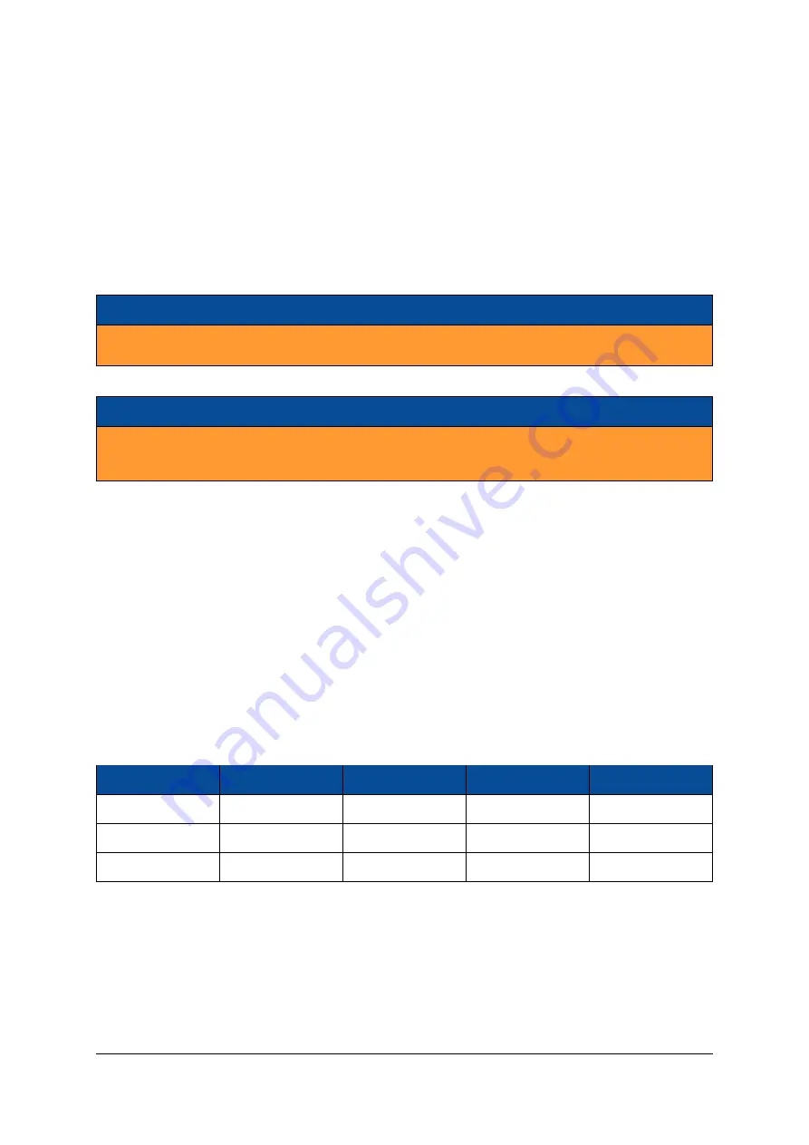
Table 42 describes the signals of the I2C interface - the pins are connected to the PS. All signals have on-
board pull-up resistors to VCC_3V3.
All signals must be connected to open collector outputs and must not be driven high from any source.
I2C_INT# is an input to the MPSoC and must not be driven from the MPSoC device.
Starting with revision 2 modules, the I2C bus is connected to both PS and PL sides (and not only to the
PS), to offer extra flexibility and help on future development. I2C on PL side is functional only when the
VCC_IO_B66 voltage is 1.8 V.
Level shifters are used between the I2C bus and MPSoC pins, as I/O banks 500 and 66 are supplied with 1.8
V. Please make sure that all pins are configured correctly and no pull-down resistors are enabled.
Signal Name
PS Pin
PL Package Pin
Connector Pin
Resistor
I2C_SDA
MIO11
Y7
A-113
2.2 k
Ω
pull-up
I2C_SCL
MIO10
V3
A-111
2.2 k
Ω
pull-up
I2C_INT#
MIO12
-
A-115
1.9 k
Ω
pull-up
Table 42: I2C Signal Description
4.3
I2C Address Map
Table 43 describes the addresses for several devices connected on I2C bus.
D-0000-428-001
57 / 66
Version 13, 15.08.2019


