Page 7
Printing and typographical errors reserved.
ELECTRONIC ASSEMBLY reserves the right to change specifications without prior notice.
EA eDIPTFT32-A
application example
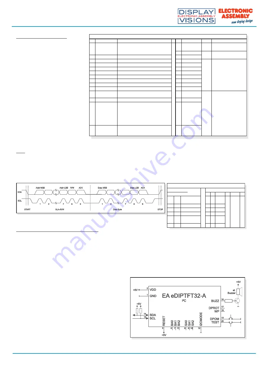
I²C-BUS INTERFACE
If the display is wired as
shown below, it can be
operated directly on an I²C
bus.
8 different base addresses
and 8 slave addresses can
be
selected on the display.
Data transfer is possible at
up
to 100 kHz. However, if
pauses of at least 100
µ
s are
maintained between the
individual bytes during
transfer, a byte can be
transferred at up to 400 kHz.
DATA TRANSFER I²C INTERFACE
principle I2C-bus transfer:
- I²C-Start
- Master-Transmit: EA eDIP-I²C-address (e.g. $DE), send smallprotocol package (data)
- I²C-Stop
- I²C-Start
- Master-Read: EA eDIP-I²C-Address (e.g. $DF), read ACK-byte and opt. smallprotocoll package (data)
- I²C-Stop
Read operation: for internal operation the
EA eDIP does need a short time before
providing the data; therefore a short pause of
min. 6µs is needed for each byte (no activity of
SCL line).
Note:
The pins BA0..2, SA0..2, DPOM, DPROT and TEST/SBUF have an internal pullup, which is why only the LO level
(0=GND) is to be actively applied. These pins must be left open for a Hi level.
On pin 20 (SBUF) the display indicates with a low level that data is ready to be retrieved from the internal send buffer.
The line can be connected to an interrupt input of the host system, for example.
Pinout eDIPTFT32-A: I2C mode
Pin Symbol In/Out Function
Pin
Symbol
In/Out Function
1
GND
Ground Potential for logic (0V)
21
GND
Ground (=Pin 1)
2
VDD
Power supply for logic (+3,3V ... +5V)
22
VDD
Power supply (=Pin 2)
3
NC
do not connect
23
AIN1
In
analogue input 0..VDD
DC impedance 1MOhm
4
NC
do not connect
24
AIN2
5
RESET
In
L: Reset
25
OUT1 / MO8
Out
8 digital outputs
maximum current:
IOL = IOH = 10mA
alternativ up to 8 matrix
keyboard output lines
(reduces the digital
output lines, see chapter
external keyboard)
6
BA0
In
Basic Address 0
26
OUT2 / MO7
7
BA1
In
Basic Address 1
27
OUT3 / MO6
8
SA0
In
Slave Address 0
28
OUT4 / MO5
9
SA1
In
Slave Address 1
29
OUT5 / MO4
10
SA2
In
Slave Address 2
30
OUT6 / MO3
11
BA2
In
Basic Address 2
31
OUT7 / MO2
12 I2CMO
In
connect to GND for I²C interface
32
OUT8 / MO1
13
DPOM
In
L: disable PowerOnMacro
do not connect for normal operation
33
IN1 / MI8
In
8 digital inputs
open-drain with internal
pullup 20..50k
alternativ up to 8 matrix
keyboard input lines
(reduces the digital input
lines, see chapter
external keyboard)
14
SDA
Bidir. Serial Data Line
34
IN2 / MI7
15
SCL
In
Serial Clock Line
35
IN3 / MI6
16
BUZZ
Out
Buzzer output
36
IN4 / MI5
17 DPROT
In
L: Disable Smallprotokoll
do not connect for normal operation
37
IN5 / MI4
18
DNC
Out
L: internal, do not connect
38
IN6 / MI3
19
WP
In
L: Writeprotect for DataFlash
39
IN7 / MI2
20
TEST
SBUF
IN
Out
open-drain with internal pullup 20..50k
IN (Power-On) L: Testmode
OUT L: data in sendbuffer
40
IN8 / MI1
all pins open: Write $DE
Read $DF
I²C - Address
Pin 11,7,6
Base
address
I²C address
BA2 BA1 BA0
D7
D6
D5
D4
D3
D2
D1
D0
L
L
L
$10
0
0
0
1
S
A
2
S
A
1
S
A
0
R
W
L
L
H
$20
0
0
1
0
L
H
L
$30
0
0
1
1
L
H
H
$40
0
1
0
0
H
L
L
$70
0
1
1
1
H
L
H
$90
1
0
0
1
H
H
L
$B0
1
0
1
1
H
H
H
$D0
1
1
0
1


