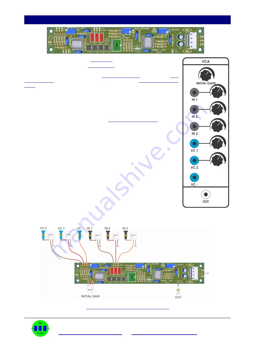
CGS364 VCA
ELBY Designs - Laurie Biddulph
9 Follan Close, Kariong, NSW 2250, Australia
2 of 3
Constructors should refer to the printed
along with the
Bill of Materials
for the current value of all components and
Notes
for general PCB assembly guidelines.
The SIGNAL inputs are, by default, AC coupled and so are only suited to audio
type signals. If you wish to control CV type signals then replace the relevant input
capacitors (C3, C4 and/or C5) with a wire link.
The CGS364 requires a matched NPN transistor pair in the Amplifier Stage at Q5
for optimum performance. Please refer to
for further
details.
Calibration
P3 [OFFSET] is used to set the DC offset of the output to zero. P2 [CV REJECT]
is used to null out the effect of the control voltage on the output.
If fitted, set P4 [INITIAL GAIN] to 0V (fully CCW).
Connect a varying waveform of low frequency (triangle wave from an LFO is ideal)
into the [CV 1] input of the VCA, and turn the associated level pot to maximum.
Connect the output of the VCA to a control voltage input of a VCO. Monitor the
output of the VCO. You should now be able to adjust these trimmers so that there
is no modulation present on the output, and the output is at zero volts. Note that
these trimmers interact to some extent, so you will need to alternately adjust
them until the best result is obtained.
P1 [CV INIT] is used to set the VCA to zero gain at 0 volts CV input. Feed an
audio signal into the [CV 1] input, and monitor the output. With no CV at any of the inputs, and the optional
external [INITIAL GAIN] pot, if used, set to its zero position, adjust this until no signal is heard.


