
eSE Series
Pad Diagrams (V1.1) 01.17.2005
•
1
(These diagrams are subject to change without further notice)
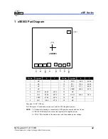
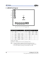
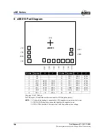
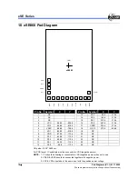
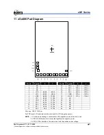
1 eSE003 Pad Diagram
VSSD
OSCI
(0,0)
eSE003
5
6
7
8
9
10
11
12
14
P2.
0
P2.
1
VD
D
VO1
VSSC
VO2
VC
C
Pin No.
Symbol
X
Y
Pin No.
Symbol
X
Y
1 NC
9 VDD
63.5
-365.2
2 NC
10 P2.1
192.4
-383.4
3 NC
11 P2.0
317.1
-383.4
4 NC
12
VSSD
460.0
-367.1
5 VCC
-458.9
-397.9 13 NC
6
VO2 -338.9 -397.9
14 OSCI 459.0 381.4
7 VSSC
-218.9
-397.9 15 NC
8 VO1
-98.9
-377.9 16 NC
Chip size
:
1180 * 1100
µ
m
For PCB layout, IC substrate must be connected to VSS (negative power).
NOTE:
1. VO should be floating or connected to VDD (positive power) when not in use.
2. VSSD & VSSC should be connected together with negative power.
3. VCC & VDD should be of the same level with the positive power voltage.