30
Design Issues
ground is anywhere within the common ground area around the off-board
connections.
For a 4-layer PCB, the ground plane serves to distribute ground from the
center of the star ground out to the various function blocks in the
floorplan. For a 2-layer PCB, ground pours should be placed on the
bottom layer (and also on the top layer where possible) in order to connect
the grounds of the various function blocks to the center of the star
ground.
EMC Keepout Area:
The area around the FT 5000 Control Module network
connection traces (from pins 25 and 26 of the
JP1
header) and associated
components should be considered “ESD Hot”. Other traces and
components (and inner planes) should be kept at least 3.5 mm (0.14 inch)
away from the network connection traces and components to prevent
ESD arc-overs. In addition, digital signal traces (and other high-speed
switching signal traces) should be routed around this keep out area. If
you route signals under this area, be sure to add a return plane (ground
or power) between the network connection trace layer and the other
signal layers.
The PCB layout should be designed so that substantial ESD hits from the
network discharge directly to the star-ground center point.
The PCB layer ground at the center of the star-ground should have a low-
inductance return to an external metal package if there is one. If there is
no metal package, then this ground area should connect to the ground
areas near the power supply connector and the external I/O connectors,
as applicable.
Ground Planes:
As ground is routed from the center of the star out to the
function blocks on the board, planes or very wide traces should be used to
lower the inductance (and therefore the impedance) of the ground
distribution system.
Host Microprocessor Kept Away From Network Connection:
The
(optional) host microprocessor (for a ShortStack device) is a potential
source of digital noise that could cause radiated EMI problems if that
noise is allowed to couple onto the external network, power, or I/O wiring.
To help prevent this coupling, the host microprocessor and any other
noisy digital circuitry should be kept away from the network side of the
FT 5000 Control Module. For example, place the host microprocessor on
the opposite side of the FT 5000 Control Module from the network, power,
and I/O connectors.
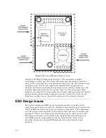
on page 31 shows a simplified view of a PCB layout for the FT 5000
Control Module. In the figure, the center of the star ground is shown as a short
standoff that would connect to the device’s enclosure.
Variations on this suggested PCB layout are possible as long as the general
principles discussed in this chapter are followed. Through-hole capacitors and
diodes can be used, but SMT components are generally superior because of their
lower series inductance.
Содержание LONWORKS FT 5000
Страница 1: ...LONWORKS Twisted Pair Control Module User s Guide 078 0015 01F...
Страница 18: ...10 Mechanical Considerations Figure 5 Neuron 3150 Control Module Mechanical Footprint...
Страница 20: ...12 Mechanical Considerations Figure 8 Vertical Component Profile for the Control Modules...
Страница 22: ......
Страница 26: ......
Страница 34: ......
Страница 55: ...www echelon com...

