


Chengdu Ebyte Electronic Technology Co., Ltd.
Copyright ©2012–2019
,
Chengdu Ebyte Electronic Technology Co., Ltd.
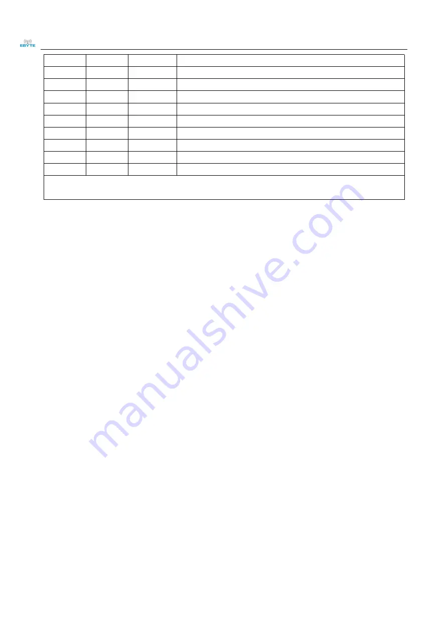
11
BUSY
Output
Used for status indication (see LLCC68 manual for details)
12
MISO
Output
SPI data output pin
13
MOSI
Input
SPI data input pin
14
NSS
Input
Module chip select pin for starting an SPI communication
15
SCK
Input
SPI clock input pin
16
GND
-
Ground wire, connected to the power reference ground
17
NC
-
-
18
DIO3
Input/Output
Configurable general-purpose IO port (see LLCC68 manual for details)
19
DIO2
Input/Output Configurable general-purpose IO port (see LLCC68 manual for details)
20
DIO1
Input/Output Configurable general-purpose IO port (see LLCC68 manual for details)
For the pin definition, software driver and communication protocol of the module, please refer to the official
LLCC68 Datasheet of SEMTECH
4 Basic Operation
4.1 Hardware Design
It is recommended to use a DC stabilized power supply. The power supply ripple factor is as small as possible and
the module needs to be reliably grounded;
Please pay attention to the correct connection of the positive and negative poles of the power supply,
reverse connection may cause permanent damage to the module;
Please check the power supply to ensure that between the recommended supply voltage, if exceeding the maximum,
the module will be permanently damaged;
Please check the stability of the power supply. Voltage can not fluctuate greatly and frequently;
When designing the power supply circuit for the module, it is often recommended to reserve more than 30% of the
margin, so the whole machine is beneficial for long-term stable operation;
The module should be as far away as possible from the power supply, transformers, high-frequency wiring and other
parts with large electromagnetic interference;
Bottom Layer High-frequency digital routing, high-frequency analog routing, and power routing must be avoided
under the module. If it is necessary to pass through the module, assume that the module is soldered to the Top Layer,
and the copper is spread on the Top Layer of the module contact part(well grounded), it must be close to the digital
part of the module and routed in the Bottom Layer;
Assuming the module is soldered or placed over the Top Layer, it is wrong to randomly route over the Bottom Layer
or other layers, which will affect the module's spurs and receiving sensitivity to varying degrees;
It is assumed that there are devices with large electromagnetic interference around the module that will greatly
affect the performance. It is recommended to keep them away from the module according to the strength of the
interference. If necessary, appropriate isolation and shielding can be done;
Assume that there are traces with large electromagnetic interference (high-frequency digital, high-frequency analog,
power traces) around the module that will greatly affect the performance of the module. It is recommended to stay
away from the module according to the strength of the interference.If necessary, appropriate isolation and shielding
can be done;
It is not recommended to use 5V level for communication lines, and there is a risk of damage. A level conversion