background image

www.dfi.com

Q7X-151 (R.D1)

Chapter 2


- Hardware Installation

16

USB Ports

The USB device allows data exchange between your computer and a wide range of simultane-

ously accessible external Plug and Play peripherals.


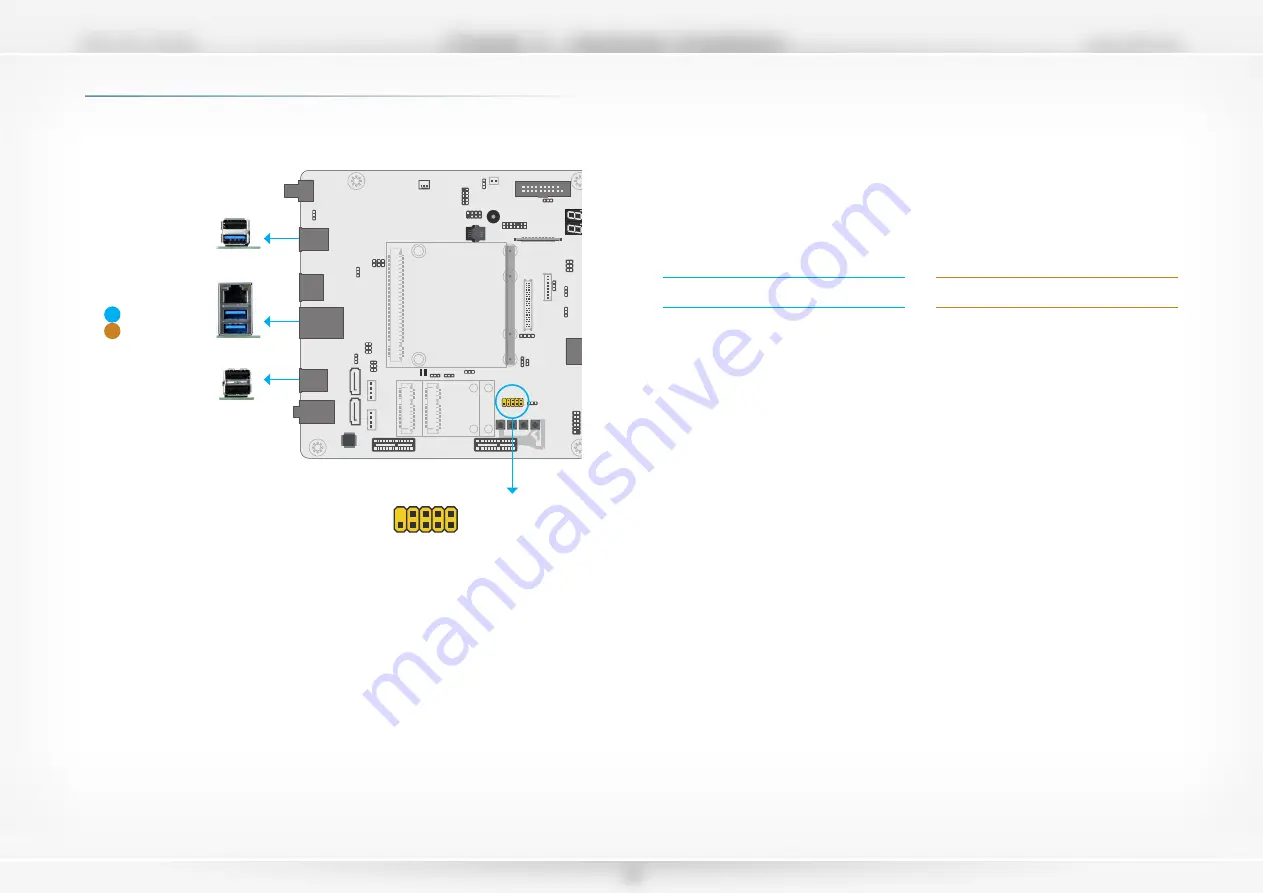
The system board is equipped with three onboard USB 3.0 ports (USB 0/1/2) and three on-

board USB 2.0 type A ports (USB 3/4/5). The 10-pin internal headers allow for 2 additional 

USB 2.0 ports (USB 6/7). 

The internal USB pin headers may be connected to a card-edge bracket. Install the card-edge 

bracket to an available slot at the rear of the system chassis and then insert the USB port 

cables to a connector.

USB 2.0 / USB 3.0 signal switch

According to the maximum number of USB 2.0 and USB 3.0 ports supported by different 

Qseven modules, this carrier board is designed with two numbers of USB ports configurable as 

listed below.

USB 3.0 (USB 0)

USB 3.0 (USB 2)

USB 2.0 (USB 5)

USB 2.0 (USB 4)

10

VCC

-Data

+Data

GND

Ke

y

VCC

-Data

+Data

GND

N. 

C.

9

1

2

USB 2.0 

(USB 6/7)

USB 3.0 (USB 1)

USB 2.0 (USB 3)

Wake-On-USB Keyboard/Mouse

The Wake-On-USB Keyboard/Mouse function allows you to use a USB keyboard or USB mouse 

to wake up a system from the S3 (STR - Suspend To RAM) state. To use this function:

Jumper Settings

USB power and USB 2.0 / USB 3.0 signal switch are configured via jumper settings as previ-

ously instructed in this chapter. 

Driver Installation

You may need to install the proper drivers in your operating system to use the USB device. 

Refer to your operating system’s manual or documentation for more information.

JP4

USB 4/5

(USB 2.0)

Rear Port A

1-2 On

Enabled

USB 2.0

2-3 On 

(default)

Disabled

USB 3.0 

JP3

USB 6/7

(USB 2.0)

Rear Port B

1-2 On

Enabled

USB 2.0

2-3 On 

(default)

Disabled

USB 3.0 

A
B


Panel I/O Ports

Содержание Qseven Q7X-151 R.D1

Страница 1: ...A54900939 Q7X 151 R D1 Qseven Carrier Board User s Manual ...

Страница 2: ...rs FCC and DOC Statement on Class B This equipment has been tested and found to comply with the limits for a Class B digital device pursuant to Part 15 of the FCC rules These limits are designed to provide reason able protection against harmful interference when the equipment is operated in a residential installation This equipment generates uses and can radiate radio frequency energy and if not i...

Страница 3: ...er Select 11 Dimming Mode Select 11 BIOS Boot Select 12 ATX AT Power Select 12 LPC GPIO Switch 13 High low Switch for MXM Pin 27 13 Panel I O Ports 14 Rear Panel I O Ports 14 Front Panel I O Ports 14 12V DC in 14 RJ45 LAN Port 15 DisplayPort 15 USB Ports 16 Audio 17 Internal I O Connectors 18 SMBus Connector 18 Front Panel 18 Cooling Fan Connectors 19 CAN Bus Connector 19 LVDS LCD Panel Connector ...

Страница 4: ...mponents or devices even before installing them in your system unit Static electrical discharge can damage computer components without causing any signs of physical damage You must take extra care in han dling them to ensure against electrostatic build up 1 To prevent electrostatic build up leave the system board in its anti static bag until you are ready to install it 2 Wear an antistatic wrist s...

Страница 5: ...iffer in accordance with the sales region or models in which it was sold For more information about the standard package in your region please contact your dealer or sales representative Before Using the System Board Before using the system board prepare basic system components If you are installing the system board in a new system you will need at least the following internal components A CPU Mem...

Страница 6: ...nnel LVDS 1 eDP port 2 DP port Audio Realtek ALC886 5 1 channel High Definition Audio Audio outputs Mic in Center Subwoofer Line in Surround and Line out USB 3 USB 3 0 and 8 USB 2 0 ports Storage 2 SATA 3 0 port with data transfer rate up to 6Gb s SATA port provides adequate space for SATA DOM Fron Pane I O 1 DP port Rear Panel I O 1 12V DC in jack 2 DB 9 RS232 serial ports 1 DP port 1 RJ45 LAN po...

Страница 7: ...id Sleep Power SD card Bottom Side Reset JP11 JP23 JP21 Front Panel SATA 0 SATA Power 0 SMBus I2 C Thermal Trip LED GPO LED PCIe 2 PCIe x1 PCIe 1 PCIe x1 JP25 JP10 JP5 SATA 1 SATA Power 1 JP3 JP4 SPI Flash BIOS DIO JP24 JP2 Realtek ALC888 eDP J9 JP12 LPC Important Electrostatic discharge ESD can damage your board pro cessor disk drives add in boards and other components Perform installation proced...

Страница 8: ... or user password c failure to start the system due to BIOS mis configuration it is suggested that the system be reconfigured with default values stored in the ROM BIOS To load the default values stored in the ROM BIOS please follow the steps below 1 Power off the system and unplug the power cord 2 Put a jumper cap on JP9 s pin 2 and pin 3 Wait for a few seconds and set JP9 back to its default set...

Страница 9: ...s JP3 JP4 as listed and illus trated below USB Power Select USB Signal Select JP10 JP4 USB 6 7 USB 2 0 JP3 USB 4 5 USB 2 0 A B JP23 JP1 JP2 2 3 On 5V_standby 2 3 On One USB 3 0 default 1 2 On 5V default 1 2 On Three USB 2 0 physical ports 3 2 1 3 2 1 3 2 1 3 2 1 JP4 USB 4 5 USB 2 0 Rear Port A 1 2 On Enabled USB 2 0 2 3 On default Disabled USB 3 0 JP3 USB 6 7 USB 2 0 Rear Port B 1 2 On Enabled USB...

Страница 10: ... the panel may result in serious damage Important Before powering on the system make sure that the power setting of JP16 match es the specification of the backlight control Supplying an incorrect voltage to the panel backlight may result in serious damage Backlight Power Select JP16 is for selecting the backlight power voltage 5V or 3 3V 1 2 On 12 5 6 On 3 3V default 3 4 On 5V 1 2 3 4 5 6 1 2 3 4 ...

Страница 11: ...LCD Inverter Power 2 3 On 5V default 2 3 On Voltage Mode 1 2 On 12V 1 2 On PWM Mode default 3 2 1 3 2 1 3 2 1 3 2 1 Dimming Mode Select JP11 is for selecting the mode for lightness control of the LVDS panel PWM Mode or Voltage Mode Important Please make sure the mode PWM or Voltage is configured according to the mode of your panel Jumper Settings Jumper Settings ...

Страница 12: ...lecting the BIOS boot source carrier board or Qseven module JP12 is for selecting the ATX AT power 5V 5V_standby or N C 1 2 Off Boot from Module SPI BIOS 1 2 On Boot from Carrier Board SPI BIOS 2 1 2 1 J9 JP12 5 6 On N C 1 2 3 4 5 6 3 4 On 5VSB 1 2 3 4 5 6 1 2 On 5V 1 2 3 4 5 6 Jumper Settings Jumper Settings ...

Страница 13: ...4 is for switching between LPC or GPIO DIO signals JP25 is for switching between high and low voltage of the battery low General Purpose Input GPI pin pin 27 of the MXM connector JP24 JP25 2 3 On LPC default 2 3 On Low 1 2 On GPIO 1 2 On High 3 3V default 3 2 1 3 2 1 3 2 1 3 2 1 Jumper Settings Jumper Settings ...

Страница 14: ...apter with 12V DC output voltage Using a volt age higher than the recommended one may fail to boot the system or cause damage to the system board 12V DC in USB 3 0 Note Line out Mic in Line in USB 2 0 Note LAN DP DC in USB 3 0 USB 2 0 DC in DP Front panel I O port 1 DP port Note The two USB 3 0 rear ports under the LAN port can act 1 as a single USB 3 0 port with additional USB 2 0 ports disabled ...

Страница 15: ...uter monitor It is used to transmit audio and video simultaneously The interface which is devel oped by VESA delivers higher performance features than any other digital interface DisplayPort DisplayPort RJ45 LAN Port The onboard RJ45 LAN port allows the system board to connect to a local area network by means of a network hub LAN Panel I O Ports Panel I O Ports ...

Страница 16: ...arrier board is designed with two numbers of USB ports configurable as listed below USB 3 0 USB 0 USB 3 0 USB 2 USB 2 0 USB 5 USB 2 0 USB 4 10 VCC Data Data GND Key VCC Data Data GND N C 9 1 2 USB 2 0 USB 6 7 USB 3 0 USB 1 USB 2 0 USB 3 Wake On USB Keyboard Mouse The Wake On USB Keyboard Mouse function allows you to use a USB keyboard or USB mouse to wake up a system from the S3 STR Suspend To RAM...

Страница 17: ...onnect any audio devices such as Hi fi set CD player tape player AM FM radio tuner synthesizer etc Line out Jack Lime This jack is used to connect a headphone or external speakers Mic in Jack Pink This jack is used to connect an external microphone BIOS Setting Please refer to the manuals of a compatible Qseven module mounted on the carrier board for more information on BIOS settings Panel I O Por...

Страница 18: ... in the S3 STR Suspend To RAM state it will blink at 4 second intervals ATX SW ATX Power Switch This switch is used to power on or off the system Front Panel Pin Assignment Pin Assignment Pin Assignment 1 N C PWR LED 2 LED Power HD LED 3 HDD Power 4 LED Power 5 Signal 6 Signal RESET 7 Ground ATX SW 8 Ground 9 Signal 10 Signal 11 N C 12 Front Panel SMBus Connector The SMBus System Management Bus co...

Страница 19: ...can be programmed to a maximum of 1Mbit s To connect the CAN controller module to the CAN bus it is necessary to add transceiver hardware When communicating in a CAN network individual message objects are configured The mes sage objects and the identifier masks for the receive filter for the received messages are stored in the message RAM Controller Area Network CAN or CAN bus is a message based p...

Страница 20: ... Pin Function Pin Function 1 GND 2 GND 3 LVDS_Out3 4 LVDS_Out7 5 LVDS_Out3 6 LVDS_Out7 7 GND 8 GND 9 LVDS_Out2 10 LVDS_Out6 11 LVDS_Out2 12 LVDS_Out6 13 GND 14 GND 15 LVDS_Out1 16 LVDS_Out5 17 LVDS_Out1 18 LVDS_Out5 19 GND 20 GND 21 LVDS_Out0 22 LVDS_Out4 23 LVDS_Out0 24 LVDS_Out4 25 GND 26 GND 27 LVDS_CLK1 28 LVDS_CLK2 29 LVDS_CLK1 30 LVDS_CLK2 31 GND 32 GND 33 LVDS_DDC_CLK 34 N C 35 LVDS_DDC_DAT...

Страница 21: ... the manuals of a compatible Qseven module mounted on the carrier board for more information on BIOS settings SATA Serial ATA Connectors SATA Serial ATA Power Connectors The SATA power connectors supply power to the SATA drive Connect one end of the provided power cable to the SATA power connector and the other end to your storage device SATA 0 SATA 3 0 SATA Power 0 SATA 1 SATA 3 0 SATA Power 1 7 ...

Страница 22: ...gnment Pin Assignment 1 L_CLK 2 L_LAD1 3 L_RST 4 L_LAD0 5 L_FRAME 6 3 3V 7 L_LAD3 8 GND 9 L_LAD2 10 11 INT_SERIRQ 12 DEBUG_48M_CLK 13 5VSB 14 5V The 1 channel I2 C bus interface conforms to the version 2 1 I2 C bus specification It operates as a master or slave device and supports a multi master bus I2 C Connector 3 3V GND I2 C_Clock I2 C_DATA NC 1 2 5 I2C Pin Assignment Internal I O Connectors In...

Страница 23: ...sized 52 pin Mini PCIe card Mini PCIe card is a small form factor PCIe card with the same signal protocol electrical definitions and configura tion definitions as the conventional PCIe SDIO Slot This expansion port is used to insert a Secure Digital Input Output SDIO or Multimedia Card MMC device Aside from storing data files a SDIO card is also capable of storing powerful software applications SD...

Страница 24: ...tch on card is aligned to the key on the socket mSATA Half Size Mini PCIe Socket Key Stand off Notch Internal I O Connectors Please follow the steps below to install the card into the socket Step 2 Press the end of the card far from the socket down until against the stand off Step 3 Screw tight the card onto the stand off with a screw driver and a stand off screw until the gap between the card and...

Страница 25: ...ction of the GPO signal is dependent on the design of the Qseven module Please refer to the pin definition of the Qseven module for more information Switches Lid turn the LVDS panel on or off Sleep set the system to sleep or wake up mode Power power on or off the system Reset reset the system Reset Power Lid Sleep Note The Sleep and Lid functions are supported only when your operating system sup p...

Страница 26: ...incorrectly installed Replace only with the same or equivalent type recommended by the manufacturer Dispose of used batteries according to local ordinances Battery Connect to the battery connector MXM Socket Battery 1 3 3V GND 2 Battery MXM Connector The MXM connector is used to interface the carrier board with a Qseven R2 1 compatible mod ule Refer to the table in the following page for the pin f...

Страница 27: ..._DAT LVDS_DID_DAT 127 GP2_I2C_CLK LVDS_DID_CLK 129 CAN0_TX 131 DP_LANE3 TMDS_CLK 133 DP_LANE3 TMDS_CLK 135 GND 137 DP_LANE1 TMDS_LANE1 139 DP_LANE1 TMDS_LANE1 141 GND 143 DP_LANE2 TMDS_LANE0 145 DP_LANE2 TMDS_LANE0 147 GND 149 DP_LANE0 TMDS_LANE2 151 DP_LANE0 TMDS_LANE2 153 HDMI_HPD 155 PCIE_CLK_REF 157 PCIE_CLK_REF 159 GND 161 PCIE3_TX 163 PCIE3_TX 165 GND 167 PCIE2_TX 169 PCIE2_TX 171 UART0_TX 1...

Страница 28: ...from the website download page at https www dfi com DownloadCenter 1 Setup is now ready to install the audio driver Click Next 2 Follow the remainder of the steps on the screen clicking Next each time you finish a step 3 Click Yes I want to restart my computer now then click Finish Restarting the system will allow the new software installation to take effect Realtek Audio Drivers To install the dr...

Страница 29: ...29 Adobe Acrobat Reader 9 3 To install the reader click Adobe Acrobat Reader 9 3 on the main menu 1 Click Next to install or click Change Destination Folder to select another folder 2 Click Install to begin installation 3 Click Finish to exit installation ...

Отзывы:

Похожие инструкции для Qseven Q7X-151 R.D1