background image


/Kits/1296-144CK.doc   


   8/15/2011


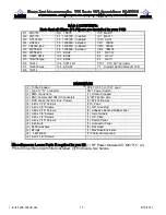
The hardware should be sorted and identified.  There are some extras.  But remember, No 
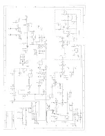
substitutions or you are on your own!!  Review the schematic and the component placement 
diagram.  Read through all of the assembly steps 1 - 13.  Identify every component used.  This will 
ensure that you have the correct tools and supplies required to complete the transverter.  It is also 
time to make the last minute decision on building the kit or not.  A full exchange towards a 
assembled version will be provided if you do not go past this step.  We want you to be on the band 
and operating not struggling to assemble this because you were not aware of the effort and 
techniques required takes to assemble this transverter! 
 

At this time you may want to mark the component placement diagram with the associated 

component values by the designators. Simply transpose the component list values to the 
component placement document. We do not do this because the values will change over time 
depending on availability, engineering changes, or obsolesces. The component list is easier to 
update and maintain providing all users the latest improvements or changes to the design. 
Updates to the design will be maintained on the DEMI web site in the future.   Now! Start the 
assembly! 


1.  Install all bottom side components of the PCB.  K1-K3, Q1, and Q2.  Do not solder the 

cans of Q1 and Q2. All 5 filters are already installed and adjusted!  
 

2.  Install all active surface mount active components, Q3, IC1- IC3, IC5- IC7, and IC10 on 

the top side of the circuit board per the top side component placement diagram.  Do not install IC4, 
VR1-VR4, or D1-D9  
 

3.  Install all surface mount capacitors and resistors and L31 per the topside component 

placement diagram.  Review the assembly tips if necessary pertaining to multiple components 
sharing the same pad.  Be sure of the placement of C57and C59.  They are dependent of the 
configuration of the transverter you require.  Common antenna port (C57 and C59) or split transmit 
and receive (C57A and C59A). 
 

4.  Wind inductors L1, L3, L9 and L10 as specified in the Bag 3 parts list.  Then install all 

inductors L1-L31.  L5 or L5A placement is dependent on the placement of C59.  The molded 
chokes L2, and L30 should be surface mounted. L12 is optional and should be installed if you wish 
to activate the PTT circuit through your Transceiver’s IF cable. 
 

5. Now install all left over leaded components, pots, resistors, capacitors, diodes, Q4 and 

regulators.  

Do not install IC4, IC9, Y1, SW1, PTC1, R22, C72, or the LED’s. Do a surface mount 

installation of C49, VR3, VR4, R25, R24, R10, R18, D2, D3, D8, and D9. When soldering the 
leaded surface mount components, do not allow solder to leak through the ground plane of the 
PCB.  It will pool up and interfere with the pallet assembly.  If you have a question, place the PCB 
on the pallet to check. 
 

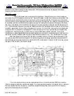
6.  Install the crystal as shown in Figure 6.  Do not install the PTC1.  It will occur later in the 

assembly instruction after testing.  The top side component placement shows the crystal standing 
up but lay it down over L2 as shown in this pictorial.  Again, do not install the PTC. 


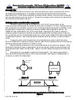
CRYSTAL

Solder Wire to
Ground and Xtal

 9Volt Supply

Xtal leads

~ 1/8” Space between
 PC Board and Xtal


Figure 6.  Crystal and PTC-60 installation detail. 

Содержание 1296-144 CK

Страница 1: ...relay on the RF side with provisions for external switching for adding a high power amplifier or preamplifier to your 23 cm system The 144 MHz IF levels and options are adjustable on both transmit and...

Страница 2: ...le helical filter that allows approximately 30 MHz of amplified bandwidth This signal is then amplified by a high level MMIC before being filtered by the next 3 pole helical filter that restricts the...

Страница 3: ...t a small tool such as a small bladed screw driver can be used to flatten them before attempting to solder See Figure 2 After verifying that the leads are flat to the surface you will be ready to sold...

Страница 4: ...ly As an alternate method you can insert one component at a time in the correct mounting location and gently push down to the circuit board while holding the component flip over the circuit board and...

Страница 5: ...ist Bag 1 Bag 4 Each side of the printed circuit board PCB is also shown to eliminate mirror image assembly errors The top and bottom side assembly operation should always begin by aligning the PCB ou...

Страница 6: ...de of the circuit board per the top side component placement diagram Do not install IC4 VR1 VR4 or D1 D9 3 Install all surface mount capacitors and resistors and L31 per the topside component placemen...

Страница 7: ...place 10 Find the bottom half of the enclosure the one with the holes in it and line up the pallet with the mounting holes Insert any two 4 40 x 7 16 screws and start them Install 2 flat head screws i...

Страница 8: ...Installed IF Connections Common or Split Start the Testing Procedure 1 All of the initial testing of the transverter is done with the pallet assembly only Before you start verify that all components...

Страница 9: ...ve the mentioned test equipment install the mixer after verification of the RX voltages If you have an mW meter connect a coax pigtail to the open pad on C17 This will be the LO circuit s output and t...

Страница 10: ...ge is out of tolerance verify all surrounding components and recheck bottom side wiring Remember MMICs draw a specified amount of current but may be a bit out of tolerance LOCATION TX VOLTAGE Matrix r...

Страница 11: ...high in frequency or to low If it is to high remove the LO shield and compress the L1 inductor and readjust C2 If the frequency is to low spread the coil slightly and re adjust C2 If the frequency is...

Страница 12: ...a non hostile RF environment If your LNA is a ultra low noise unit it most likely will not have the IP3 performance the transverter has It will overload before any component in the transverter will So...

Страница 13: ...pen and NC normally closed The C connection can be wired to ground or positive voltage such as the source 13 8 VDC The K2 common connection will then be toggled depending on what state the transverter...

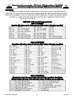
Страница 14: ...fied C1 0 01 F C20 100 C39 33 C60 0 3 3 VAR C2 1 4 Piston C21 18 C40 0 1 F C61 0 1 F 1008 C3 0 01 F C23 18 C41 33 C62 0 1 F 1008 C4 18 C24 100 C42 33 C63 33 C5 22 C25 0 01 F C43 0 1 F C64 33 C6 0 01 F...

Страница 15: ...HC 18 U D8 1N914 HARDWARE 2 1000 F leaded R36 THC 50 10 W Load 1 Type N connector SW1 Power Switch 2 SMA connectors 1 Shield Prepped 2 BNC Female UG1094 U Connectors 3 18 Teflon wire 3 RCA Jacks Contr...

Страница 16: ......

Страница 17: ...o o o o o o o r o o o o o o o o o BB 6 6 o RR 5 5 o o o o o o o o o o o o o o O u ololo l n l i a l f lYto I Xlrxo o o l L l ooo t o o o o o o o o o o o o o P lo o t l Fc 1 of AS o o o o o ol S o o x...

Страница 18: ...o o o o o o o ru LN o o C o o 1 d o o o J T X L o o o L l k l o o a n 1 l v ff t o o o o 0 e 1Jfl L4 lo o o e s i o 1T I l to3 alf llll UdC AlEl l SSU 99 U b F I q6 _ I 1 Y o o o O O o o o o o o o l...

Отзывы: