background image


6-8


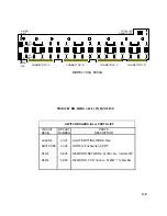
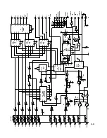
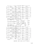
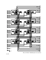
NTERFACE BOARD

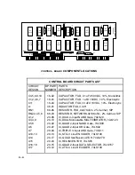
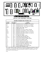
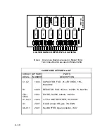
 COMPONENT LOCATIONS 


INTERFACE BOARD CIRCUIT PARTS LIST 

 CIRCUIT 

DP PART   

PARTS 

 DESIGN. 

NUMBER   

DESCRIPTION 

 C1-7 

16-02 

 CAPACITOR, FXD, .01 uFd 50VDC, 10%, Monolithic 

 C8 

18-04 

 CAPACITOR, FXD, .33 uFd 10VDC, 10%, Tantalum 

 C9-12 

18-02 

 CAPACITOR, FXD, 3.3 uFd 15 VDC, 10%, Tantalum 

 CR1-4 

22-01 

 DIODE, 50VPIV, 200mA, 1N4150 

 L1 

46-01 

 INDUCTOR,FXD,4.7uH 

 R1-4 

69-03 

 RESISTOR, FXD, 1Kohm, .0125W, 1% Met film 

 R5-6 

69-05 

 RESISTOR, FXD, 49.9Kohm, .0125W, 1% Met film 

 RN1,2 

68-02 

 RESISTOR, NETWORK,7x10Kohm, 2% Cermet,SIP 

 RN3,4 

68-04 

 RESISTOR, NETWORK,8x6.2Kohm, 2% Cermet,SIP 

 S1 

31-05 

 SWITCH,SIP,6 Position 

 S2 

50-11 

 CONNECTOR HEADER, 3 Posts 

 U1-3 

20-18 

 IC,QUAD D-Type FLIP-FLOP, LS379 

 U4,7,10 

20-05 

 IC,HEX Schmitt Trigger INVENTOR,, LS14 

 U5 

20-11 

 IC,QUAD 2-Input Schmitt Trig NAND, 74LS132 

 U11 

20-08 

 IC,QUAD 2-Input NAND, 74LS38 

 U13 

20-09 

 IC,DUAL D-Type FLIP-FLOP, LS74 

 U14 

20-10 

 IC,DUAL Monostable MULTIVIBRATOR, LS123 

 U8 

20-19 

 IC,8-BIT MAGNITUDE COMPARATOR, LS688 

 U9 

20-20 

 MEMORY CIRCUIT, 512x8,Programed 

 U12 

20-03 

 IC,HEX INVENTOR, Open Col. Output, LS05 

 U6 

20-16 

 IC,8-BIT SHIFT REGISTER, LS164 

Note:  The IDC Connector  jumper (switch) that can be switched to accommodate either HP Basic computers or 
PC computers.  The switch should connect the center and right pin for HPBASIC computers.  The center and 
left pin are connected for most PC’s.  (National Instruments AT-GPIB/TNT board has been found to work 
better with the switch in the HP position. 

+ 3.3

µ

F

+ 3.3

µ

F

+ 3.3

µ

F

+ 3.3

µ

F

+ 33 

µ

F

 4.7 

µ

H

1K

1K

1K

4.49K

4.49K

1K

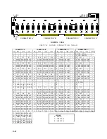
INTERFACE BOARD

320-007C

F379

U1

F379

U2

F379

U3

LS14

U4

LS123


U5

LS164


U6

LS14


U7

LS123

U14

LS74

U13

LS05

U12

LS38

U11

LS14

U10

PROM

U9

LS688

U9

BUS

ADDRESS

RN1


C2

RN3
RN4

CR1

R4

C9

R5

R6

C6

C10

C11

C12

C4

C3

C7

CR3 CR4

R3

R2

R1

CR2

RN2

C8 L1

C1

S1

S2


22-01

C5

PC  HP

Содержание 160A

Страница 1: ...OPERATING INSTRUCTIONS AND SERVICE MANUAL LOW THERMAL SCANNER MODLES 160A 164A 320A Copyright DATA PROOF 1984 1999 1177 S De Anza Blvd San Jose CA 95129 Phone 408 865 1177 Fax 408 865 1166 www DataProof com ...

Страница 2: ...l incidental or consequential damages arising out of the use of this product No other warranty is expressed or implied SAFETY PRECAUTIONS This product has been designed and tested in accordance with IEC1010 1 EN61010 1 including amendment 1 1995 for insulation category II use Use of this equipment in a manner not specified may could result in personal injury AC POWER SOURCE This product is intende...

Страница 3: ...PANEL CONNECTIONS 3 2 3 3 FRONT PANEL OPERATION 3 3 3 4 OPERATION VOLTAGE SELECTION 3 4 3 5 ADDRESS SELECTION 3 5 3 6 OPERATION FROM INTERFACE BUS 3 6 3 7 SAMPLE PROGRAMS 3 7 3 8 REMOTE LOCK 3 8 3 8 STANDARD PROTECTION FOR MULTIPLE SCANNERS 3 8 3 9 OPTION 3 SCANNER GUARD 3 8 SECTION IV THEORY OF OPERATION PACE 4 0 INTRODUCTION 4 1 4 1 LATCHING RELAY 4 1 4 2 LOW THERMAL DESIGN 4 2 4 3 SCANNER CONFI...

Страница 4: ...CH BOARD DIAGRAM 6 3 160A SWITCH BOARDS PARTS TABLE 6 4 164A SWITCH BOARDS PARTS LIST 6 5 CONTROL BOARD PARTS LIST 6 6 CONTROL BOARD DIAGRAM 6 7 BUS INTERFACE PARTS LIST 6 8 BUS INTERFACE BOARD DIAGRAM 6 9 CLOSE CIRCUIT PARTS LIST 6 10 CLOSE CIRCUIT BOARD DIAGRAM 6 11 CLEAR CIRCUIT BOARD PARTS LIST 6 12 CLEAR CIRCUIT BOARD DIAGRAM 6 13 RELAY BOARD PARTS LIST 6 14 RELAY BOARD DIAGRAM 6 15 POWER SUP...

Страница 5: ... comparing voltage reference standards as well as four terminal measurements on resistance devices Special care has been taken to minimize thermal offsets The switches used are latching relays requiring only a few milli second pulse to actuate Several systems are used to protect the devices connected to the scanner from being damaged by operator error or scanner failure It can be operated from the...

Страница 6: ...30 SCANNER CONTROL Local using front panel push buttons Remote via IEEE 488 bus interface included RELAY CONTACT RATINGS Life greater than 10 000 000 cycles at low levels Initial contact resistance 0 05 ohm maximum Current 100 milliamp maximum at 10 volts Voltage switched 100 volts maximum at 1 milliamp Voltage non switched 300 volts max for cable inputs Voltage non switched 600 volts max for term...

Страница 7: ...en This line can be connected in parallel with other scanners cascaded in a large system to protect standards from being shorted together Two systems are provided one for line A and one for line B 1 4 REFERENCE STANDARD PROTECTION SYSTEMS Three systems are used to help protect standards from being damaged due to scanner failure or operator error These systems are described briefly below See Theory...

Страница 8: ...1 4 Blank Page ...

Страница 9: ...wer transformer depending on the scanner model The jumper connections are shown on the power supply diagram WARNING BEFORE SWITCHING ON THIS INSTRUMENT THE PROTECTIVE TERMINAL OF THIS INSTRUMENT MUST BE CONNECTED TO A PROTECTIVE EARTH CONTACT THE POWER LINE CORD SUPPLIED WILL PROVIDE THE PROTECTIVE GROUNDING WHEN INSERTED INTO A SOCKET OUTLET PROVIDED WITH AN EARTH CONTACT THE PROTECTIVE ACTION MU...

Страница 10: ...2 2 Blank Page ...

Страница 11: ...ttons when depressed at the same time that either the A LINE or the B LINE push button is down will cause the corresponding relay to close 5 LINE A lights indicates which LINE A relay is closed 6 LINE B lights indicates which LINE B relay is closed 7 REMOTE light is illuminated when the scanner is in bus control The front panel push buttons are inoperative 8 LOCAL Light is illuminated when the sca...

Страница 12: ... with the black band 2 LINE A OUTPUT positive Connect to positive terminal of measuring system 3 LINE A OUTPUT COM Connect to Line B output com for voltage comparisons 4 LINE B OUTPUT positive Connect to negative terminal of measuring system 5 LINE B OUTPUT COM Connect to Line A output com for voltage comparisons 6 GND Connected to chassis at relay isothermal box 5V Max to DATA PROOF SUNNYVALE CA ...

Страница 13: ...on to reset To connect one of the channel inputs to LINE A proceed as follows a Press and hold down the LINE A push button This will cause any previously closed relay on the A LINE to be cleared b Press the numbered push button corresponding to the input to be connected This will cause the relay to actuate connecting the input line to the A output and also turn on the appropriate light c To actuat...

Страница 14: ...from the power cord receptacle on the power entry module 3 Inserted a small flat bladed tool into the slot at the left edge of the cover and carefully pry the cover off the fuse cavity 4 Grasp the white plastic voltage select board use with a small pair of pliers and pull straight outward until the voltage select board unseats from the power entry module cover to change the voltage setting Hold th...

Страница 15: ...imal Listen Talk A5 A4 A3 A2 A1 code SP 0 0 0 0 0 00 A 0 0 0 0 1 01 B 0 0 0 1 0 02 C 0 0 0 1 1 03 D 0 0 1 0 0 04 E 0 0 1 0 1 05 F 0 0 1 1 0 06 G 0 0 1 1 1 07 H 0 1 0 0 0 08 I 0 1 0 0 1 09 J 0 1 0 1 0 10 K 0 1 0 1 1 11 L 0 1 1 0 0 12 M 0 1 1 0 1 13 N 0 1 1 1 0 14 O 0 1 1 1 1 15 0 P 1 0 0 0 0 16 1 Q 1 0 0 0 1 17 2 R 1 0 0 1 0 18 3 S 1 0 0 1 1 19 4 T 1 0 1 0 0 20 5 U 1 0 1 0 1 21 6 V 1 0 1 1 0 22 7 W...

Страница 16: ...ate a relay the bus interface must first receive the correct address then a three character ASCII code designating the relay and then a carriage return line feed For example using an HPBASIC computer the statement OUTPUT 724 AO1 would cause any relay on LINE A to be cleared and then relay number 1 to be closed In this example 7 is the controller IO address 24 is the scanner address and A01 is the ...

Страница 17: ...ait of at least 200 milliseconds is required between relay actuations to allow time for the relay circuits to actuate The second program example has exactly the same result as the first program listed above but uses string output statements The formatted output statement is used to assure the first character that the scanner sees after the address is the line code and the next two characters are t...

Страница 18: ... scanner in a large system by connecting the PROTECT terminals together Both the A and B PROTECT terminals are connected to an open collector TTL gate on the control board When all relays are open the terminal will be high 5 volts through 10 kohm and when any relay is closed the terminal will be low near 0 volts Connecting either terminal to COM will prevent any relay on that line from being activ...

Страница 19: ... The device that makes this scanner possible is a sensitive latching relay originally manufactured for the telephone industry The major problem with conventional relays is the thermal offset voltage caused by the heat generated by the current in the relay coil With this latching relay a short pulse of only 10 milliseconds is all that is required to toggle the contacts from one side to the other Th...

Страница 20: ...SIGN Special care has been taken to minimize thermal offsets The switches used are latching relays requiring only a short pulse to actuate and thus no self heating occurs Gold plated fingers on the relay armature make direct contact to hard gold pads on special circuit boards Relays make connection by shorting together adjacent pads on the board with pairs of contacts Thus any thermal emf caused b...

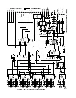
Страница 21: ...serially one ASCII character at a time This serial format is changed to a parallel format by means of a decoder ROM on the interface board as can be seen in Figure 4 4 To allow the system to operate from the front panel the push button data is converted to a form identical to binary data from the bus interface circuit A selector at this point switches between bus or push button operation A 6 to 64...

Страница 22: ...s and will complete the series protection circuit only if all the relays on the line are in the clear position Thus no relay on the A line can be closed if any other relay on the A line is already closed and similarly no B line relay can be closed if any other relay on the B line is already closed These series protection lines are brought out to terminals on the rear panel Thus if more than one sc...

Страница 23: ...ups of four units is shown in Figure 4 5 READING A LINE B LINE El Group 1 Unit 1 Group 2 Unit 1 E2 Group 1 Unit 1 Group 2 Unit 3 E3 Group 1 Unit 3 Group 2 Unit 3 E4 Group 1 Unit 3 Group 2 Unit 1 E5 Group 1 Unit 2 Group 2 Unit 2 E6 Group 1 Unit 2 Group 2 Unit 4 E7 Group 1 Unit 4 Group 2 Unit 4 E8 Group 1 Unit 4 Group 2 Unit 2 E9 Group 2 Unit 2 Group 1 Unit 1 E10 Group 2 Unit 2 Group 1 Unit 3 Ell Gr...

Страница 24: ...F 2 0 007 0 000 44 F 3 B 2 0 015 0 000 13 B 3 F 3 0 018 0 001 45 F 3 B 3 0 019 0 003 14 B 4 F 3 0 012 0 003 46 F 4 B 3 0 013 0 004 15 B 4 F 4 0 016 0 000 47 F 4 B 4 0 020 0 004 16 C 1 F 4 0 022 0 001 48 G 1 B 4 0 005 0 001 17 C 1 G 1 0 014 0 001 49 G 1 C 1 0 013 0 001 18 C 2 G 1 O 004 0 001 50 G 2 C 1 0 017 0 001 19 C 2 G 2 0 002 0 000 51 G 2 C 2 0 006 0 004 20 C 3 G 2 0 000 0 002 52 G 3 C 2 0 006...

Страница 25: ...1 Nanovoltmeter connected to the Scanner A and B high red output lines with the A and B low black output lines shorted together The Data Proof Voltage Reference Maintenance Program VoltRef was run on a computer to control the instruments to make the measurements VoltRef closes the two relays waits 20 seconds and then takes 10 readings It then reverses the relays waits another 20 seconds and takes ...

Страница 26: ...4 8 Blank Page ...

Страница 27: ...tine in any of the Data Proof software programs A less common reason for unstable readings is a relay that has drifted out of adjustment so that the contacts do not properly wipe clean A bad relay contact can be verified by moving the test unit to a different channel and trying the measurement again Another way to check for a bad relay is to short out several channels including the suspect channel...

Страница 28: ...ust be pulled out There is enough slack in the channel input lines to allow the board to be withdrawn far enough to replace the lower relays WARNING STANDARD CELLS CONNECTED TO THE SCANNER COULD BE DAMAGED DURING THE PROCESS OF EXCHANGING RELAYS IT IS RECOMMENDED THE CELLS BE DISCONNECTED FROM THE BOARD BEING WORKED ON To install a new relay on the board center the alignment pins over the holes in...

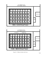
Страница 29: ...29 28 27 26 25 24 23 22 21 20 19 18 17 16 15 14 13 12 11 10 9 8 7 6 5 4 3 2 1 SPARE RELAYS 164A 6664A Rear Panel TRANSFORMER A Line Relays on Top B Line Relays on Bottom 16 15 14 13 12 11 10 9 8 7 6 5 4 3 2 1 16 15 14 13 12 11 10 9 8 7 6 5 4 3 2 1 High Relays Low Relays Figure 5 1 Relay Locations Top View ...

Страница 30: ...5 4 ...

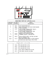
Страница 31: ...e is a circuit diagram a component location diagram and a parts list There is also a list of general parts that are located on the chassis and the rear panel 6 2 ORDERING INFORMATION To obtain parts directly from the factory contact Data Proof at www DataProof com Identify parts by their Data Proof part number Include the instrument model and serial numbers as well as the part description ...

Страница 32: ...MOUNTING BASE 4 51 04 TERMINAL BLOCK 4 CONDUCTOR Opt 1 82 09 SOLID COPPER CABLE 4 COND 22 GAGE NEC CM BELDEN 9794 Opt 3 81 12 SHIELDED TEFLON CABLE 2 COND 22GAGE Stranded silver plated copper Weico 5222 MOTHER BOARD NOT SHOWN 50 04 PC CONNECTOR 15 PIN 50 05 PC CONNECTOR 18 PIN 50 06 PC CONNECTOR 18 PIN 51 04 FLAT CABLE CONNECTOR 24 PIN 81 14 FLAT CABLE 28 AWG 24 COND 5V Max to PROTECT GP IB BUS GN...

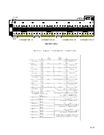
Страница 33: ...D B1 LED S33 LOCAL LED REMOTE LED S4 S2 S6 S8 S10 S12 S14 S16 S18 S20 S22 S24 S26 S28 S30 S32 B4 B6 B8 B10 B12 B14 B16 B18 B20 B22 B24 B26 B28 B30 B32 A4 A6 A8 A10 A12 A14 A16 A18 A20 A22 A24 A26 A28 A30 A32 CONNECTOR A CONNECTOR B CONNECTOR B CONNECTOR D MODEL 320A ...

Страница 34: ... B 18 S LINE B S LINE B S LINE B C S16 S16 S16 C S24 C S32 A D B16 LED B16 HIGH B16 LED D B24 LED B8 LOW D B32 LED B16 LOW B E B15 LED B15 HIGH B15 LED E B23 LED B7 LOW E B31 LED B15 LOW C S8 S8 S8 F S14 S14 S14 F S22 F S30 D B8 LED B8 HIGH B8 LED H B14 LED B14 HIGH B14 LED H B22 LED B6 LOW H B30 LED B14 LOW E B7 LED B7 HIGH B7 LED J B13 LED B13 HIGH B13 LED J B21 LED B5 LOW J B29 LED B13 LOW F S6...

Страница 35: ...1 R2 68 05 RESISTOR NETWORK 9x180 ohm Cermet SIP R3 R4 69 03 RESISTOR FXD 1Kohm 0125W 1 Met film A LINE S17 B LINE S18 A1 LED B1 LED LOCAL LED REMOTE LED S2 S1 S3 S4 S5 S6 S7 S8 S9 S10 S11 S12 S13 S14 S15 S16 B2 B3 B4 B5 B6 B7 B8 B9 B10 B11 B12 B13 B14 B15 B16 A2 A3 A4 A5 A6 A7 A8 A9 A10 A11 A12 A13 A14 A15 A16 CONNECTOR A CONNECTOR B CONNECTOR D CONNECTOR C MODEL 164A 6664A HI LOW HI LOW ...

Страница 36: ... 3 6 7 18 01 CAPACITOR FXD 1 uFd 15VDC 10 Electrolytic C11 18 04 CAPACITOR FXD 33 uFd 10VDC 10 Electrolytic L1 46 01 INDUCTOR FXD 4 7uH RN1 68 06 RESISTOR FXD 9x47Kohm 2 Cermet SIP RN2 3 4 5 6 68 03 RESISTOR NETWORK 9x10Kohm 2 Cermet SIP U1 2 20 06 IC DUAL 4 Input NAND Gate 74LS20 U3 4 9 20 10 IC DUAL Monostable MULTIVIBRATOR 74LS123 U5 8 20 02 IC QUAD 2 Input NAND Gate 74LS00 U6 20 07 IC QUAD 2 I...

Страница 37: ...6 U6 U16 LS157 SELECTOR A B 5 6 13 3 10 11 14 2 Hi Clear Hi 1 16 Hi Trig Hi A FROM BUS INTERFACE LO REMOTE HI 1 16 TO CLOSE BOARDS B SERIES LINE A SERIES LINE TO RELAY BOARDS B A B PROTECT A PROTECT TO REAR PANEL 2 1 9 K 10 L 5 6 7 4 A 1 16 B 1 16 A 17 32 B 17 32 B CLOSE A CLOSE B CLEAR A CLEAR TO CLEAR BOARD H 2 6 3 20 ms 20 ms S1 S2 S3 S4 R S 14 15 F 5 E D 6 HI CLEAR HI TRIG HI A P N 12 13 D1 D2...

Страница 38: ... IC QUAD 2 Input NAND 74LS38 U13 20 09 IC DUAL D Type FLIP FLOP LS74 U14 20 10 IC DUAL Monostable MULTIVIBRATOR LS123 U8 20 19 IC 8 BIT MAGNITUDE COMPARATOR LS688 U9 20 20 MEMORY CIRCUIT 512x8 Programed U12 20 03 IC HEX INVENTOR Open Col Output LS05 U6 20 16 IC 8 BIT SHIFT REGISTER LS164 Note The IDC Connector jumper switch that can be switched to accommodate either HP Basic computers or PC comput...

Страница 39: ... PROM U14 LS123 CLEAR DELAY U13 LS74 LISTEN F F 6 F 7 H 8 J 9 K L 11 10 M 12 N 15 HI TRIG A a 13 16 E F 5 C D P HI A 1 2 3 A B C T U 14 17 18 V 4 D RN2 10K RN2 10K RN2 10K RN2 10K RN2 10K RN2 10K CR1 6 5 2 1 4 3 8 9 10 11 4 3 12 13 9 8 6 5 3 4 13 12 11 1 2 5 6 2 1 13 12 1 2 3 11 10 4 5 6 9 8 8 10 9 1 2 3 1 2 10 9 8 4 5 6 13 12 11 3 4 11 10 6 5 9 8 Q7 Q6 Q5 Q4 Q3 Q2 Q1 Q0 P7 P6 P5 P4 P3 P2 P1 P0 G ...

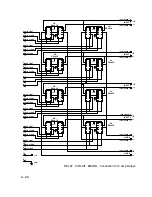
Страница 40: ...s are used in Model 160A Two Close Boards are used in Model 320A CLOSE CIRCUIT PARTS LIST CIRCUIT DP PART PARTS DESIG NUMBER DESCRIPTION C1 C2 16 02 CAPACITOR FXD 01 uFd 50VDC 10 Monolithic R1 69 03 RESISTOR FXD 1Kohm 0125W 1 Met film CR1 CR32 22 01 DIODE 50VPIV 200mA 1N4150 U1 2 4 5 20 22 3 TO 8 LINE DECODER 74LS138N U3 20 07 QUAD 2 Input OR gate 74LS32N U6 U11 20 01 Hex BUFFER Open Collector 740...

Страница 41: ...6 11 ...

Страница 42: ...el 320A OPEN CIRCUIT PARTS LIST CIRCUIT DP PART PARTS DESIG NUMBER DESCRIPTION C1 C2 16 02 CAPACITOR FXD 01 uFd 50VDC 10 Monolithic RN1 RN2 68 01 RESISTOR NETWORK 9x1 Kohm Cermet SIP R1 R2 69 03 RESISTOR FXD 1Kohm 0125W 1 Met film D1 D16 22 01 DIODE 50VPIV 200mA 1N4150 U1 2 5 6 20 21 Quad D TYPE FLIP FLOP 74LS175N U3 20 05 Hex INVERTOR 74LS14N U4 20 10 MONOSTABLE MULTIVIBRATOR 74LS123N U7 8 12 13 ...

Страница 43: ...6 13 ...

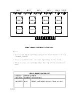
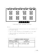
Страница 44: ...RD COMPONENT LOCATIONS Notes 1 Each Board holds latching relays for four channels of low thermal inputs 2 Four or eight boards are used depending on the model 3 These boards are located under the top of the isothermal box RELAY BOARD PARTS LIST CIRCUIT DP PART PARTS DIAGRAM NUMBER DESCRIPTION All PARTS 49 01 RELAY LATCHING 3 Pole 2 Throw 12V coil ...

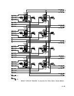
Страница 45: ...SE 4B CLOSE 15 15 15 15 15 15 15 RELAY 4A RELAY 3A RELAY 2A RELAY 1A RELAY 1B RELAY 2B RELAY 3B RELAY 4B 164A 6664A P INPUT 1 2B LIGHT 2B CLEAR 2B CLOSE 2A LIGHT 2A CLEAR 1B LIGHT 1A LIGHT 1B CLEAR 1A CLEAR 1ACLOSE 1B CLOSE 3B CLOSE 15 COM 4 D 12 N P 13 S R 14 15 K K 9 11 L 10 E H 5 7 6 F A C 1 3 2 B INPUT 2 INPUT 3 INPUT 4 LINE A LINE B 164A 6664A C 164A 6664A P 164A 6664A P 164A 6664A P 164A 666...

Страница 46: ... Hi G C P INPUT 4 Lo G C P INPUT 4 Hi G C P RELAY BOARD COMPONENT LOCATIONS Notes 1 Each Board holds latching relays for four channels of low thermal inputs 2 Four or eight boards are used depending on the model 3 These boards are located under the top of the isothermal box RELAY BOARD PARTS LIST CIRCUIT DP PART PARTS DIAGRAM NUMBER DESCRIPTION All PARTS 49 03 RELAY LATCHING Guarded 2 Throw 12V co...

Страница 47: ...6 17 ...
Страница 48: ... 15 15 RELAY 4A RELAY 3A RELAY 2A RELAY 1A RELAY 1B RELAY 2B RELAY 3B RELAY 4B HI GUARD 2B LIGHT 2B CLEAR 2B CLOSE 2A LIGHT 2A CLEAR 1B LIGHT 1A LIGHT 1B CLEAR 1A CLEAR 1ACLOSE 1B CLOSE 3B CLOSE 15 COM 4 D 12 N P 13 S R 14 15 K K 9 11 L 10 E H 5 7 6 F A C 1 3 2 B INPUT 1 HI INPUT 1 LO P LO GUARD HI GUARD LO GUARD INPUT 2 LO INPUT 2 HI C C P P P P P C C C C HI GUARD HI GUARD LO GUARD LO GUARD INPUT...

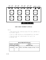
Страница 49: ...LAYS 2 AMP RELAY BOARD COMPONENT LOCATIONS Notes 1 Each Board holds latching relays for four channels of low thermal inputs 2 Four or eight boards are used depending on the model 3 These boards are located under the top of the isothermal box 2 AMP RELAY BOARD PARTS LIST CIRCUIT DP PART PARTS DIAGRAM NUMBER DESCRIPTION All PARTS 49 02 RELAY LATCHING 2 AMP ...

Страница 50: ...YS 3B RELAYS 4B RELAYS 164A 6664A P INPUT 1 2B LIGHT 2B CLEAR 2B CLOSE 2A LIGHT 2A CLEAR 1B LIGHT 1A LIGHT 1B CLEAR 1A CLEAR 1ACLOSE 1B CLOSE 3B CLOSE 15 COM D 12 P 13 S R 14 15 K K 9 11 L 10 E H 5 7 6 F A C 1 3 2 B INPUT 2 INPUT 3 INPUT 4 LINE A LINE B 164A 6664A C 164A 6664A P 164A 6664A P 164A 6664A P 164A 6664A P 164A 6664A C 164A 6664A C 164A 6664A C 164A 6664A C 164A 6664A C 164A 6664A P 15 ...

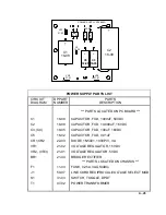
Страница 51: ...D C1 18 08 CAPACITOR FXD 1000uF 50VDC C2 18 09 CAPACITOR FXD 10 000uF 16VDC C3 C4 18 05 CAPACITOR FXD 100uF 16VDC C5 16 02 CAPACITOR FXD 0 01uF CR1 CR2 22 03 DIODE 1N5401 100VPIV 3A VR1 21 02 VOLTAGE REGULATOR 15VDC VR2 VR3 21 01 VOLTAGE REGULATOR 5VDC BR1 21 04 BRIDGE RECTIFIER PARTS LOCATED ON CHASSIS F1 11 03 FUSE 0 25A 3AG SloBlo J1 50 07 LINE CORD RECIPROCAL VOLTAGE SELECT MOD S1 31 03 SWITCH...

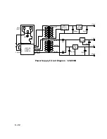
Страница 52: ... ORANGE BROWN WHITE GREEN GREEN 15V 5V 5V COM F1 J H K L GND A C D E F BR1 BRIDGE RECTIFIER VR1 15V REG VIOLET VIOLET VR2 5V REG VR3 5V REG CR1 CR2 VOLTAGE SELECT MODULE 1000µF 01µF 100µF 100µF 10 000µF Power Supply Circuit Diagram 320 006D ...

Страница 53: ...al Guarded Scanner Model Numbers 160A 164A 320A Product Options All Options Conforms to the following Product Specifications EMC EN50081 1 1992 EN55022 Class B EN50082 2 1992 IEC 801 2 1984 SAFETY EN 61010 1 1993 1995 Supplementary Information The Product herewith complies with the Sunnyvale California James A Marshall President January 10 1996 May 15 1997 Note The declaration of conformity applie...

Отзывы: