8
5. Adjustment Method
“** This Adjustments should be done by using SVC Remote Controller “”R-30SVC6”””
MICOM PROGRAMMING
-Micom should be programmed by using PC with operation tests.
-The specific s/w and adapter are needed for micom programing.
SCREEN Adjustment
(1) Press the SVC key of the SVC remote controller ( R-30SVC6)
(2) Adjust Screen Volume of FBT until the horizontal line is just disappeared.
(3) Press the Screen key on the SVC remote controller to release Screen mode.
FOCUS Adjustment
-Adjust with the Focus volume on the FBT until you get the most clear resolution of 350
line and corner of screen.
WHITE BALANCE Adjustment
(1) Measuring instrument settings
-The others are same with other chassis
-NITSUKI have to be set exactly to Reference G, CHROMA : OFF
-The Reference coordinates : HIGH ( x : 288, y : 301, Y : 100cd/m2)
LOW ( x : 288, y : 301, Y : 15cd/m2)
(2) High-Beam Adjustment
-Adjust with R DRV +/-, B DRV +/- keys so that only R,B bars in the high beam on the
instrument may be located in the center. (“G” DRIVE is Fixed.)
(3) Low-Beam Adjustment
-Adjust with R BIAS +/-, B BIAS +/- keys so that only R,B bars in the low beam on the
instrument may be located in the center. (“G” DRIVE is Fixed.)
VERTICAL CENTER Adjustment
-Pattern : RETMA
-Adjust with V-CEN +/- keys to harmonize pattern’s upper marking with Lower marking.
(ex) “2/2” or “3/3” or “1/1”
VERTICAL SIZE Adjustment
-Pattern : RETMA
-Adjust with V-SIZE +/- keys so that the upper and the lower ‘3’ marks of the RETMA
pattern may be located at the boundaries of the screen.
Horizontal Center Adjustment
-Pattern : RETMA
-Adjust with H-/- keys to harmonize the position of pattern’s Left side with
Right side.
Содержание DUA-3270GB
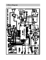
Страница 4: ...4 2 Block Diagram 1 Analog Part ...
Страница 19: ...19 7 Schametic Diagram 1 ALALOG MAIN PART ...
Страница 20: ...20 Schametic Diagram 2 POWER PART ...
Страница 21: ...21 Schametic Diagram 3 DIGITAL MAIN PART 1 ...
Страница 22: ...22 Schametic Diagram 3 DIGITAL MAIN PART 2 ...
Страница 23: ...23 Schametic Diagram 3 DIGITAL MAIN PART 3 ...
Страница 24: ...24 8 Printed Circuit Board 1 Main PCB ...
Страница 25: ...25 Printed Circuit Board 2 Power PCB ...
Страница 26: ...26 Printed Circuit Board 3 Digital PCB Top ...
Страница 27: ...27 Printed Circuit Board 4 Digital PCB Bottom ...
Страница 28: ...28 Printed Circuit Board 5 CRT PCB 6 Union PCB ...
Страница 29: ...29 9 Mechanical Exploded Diagram _ p p ª ø L fl T Œx bª Ø L fi Ø p fi Ø 9 p L ...
Страница 40: ...DAEWOO ELECTRONICS CORP PRINTED DATE JAN 2006 686 AHYEON DONG MAPO GU SEOUL KOREA C P O BOX 8003 SEOUL KOREA ...


