- 63 -
Service manual WP 895/895F, CP885/885F
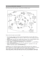
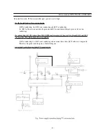
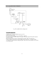
On normal run mode, I501 microcontroller pin 1 (power) is set to high
• So, I810 controlled rectifier is not conducting
- Q809 is conducting. So, Q808 is not conducting and Q807 is conducting
- So, Q807 collector is connected to the ground and I810 controlled rectifier gate pin is set to low (no
conducting)
• So, current from 14V DC voltage (from T801 SMPS transformer pin 13) does not flow through Q811 and Q810
transistors but flows through I806 IC error amplifier
- Q809 is conducting. So, Q810 is not conducting and no current flows from Q810 collector to the ground
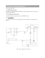
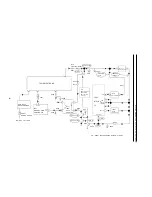
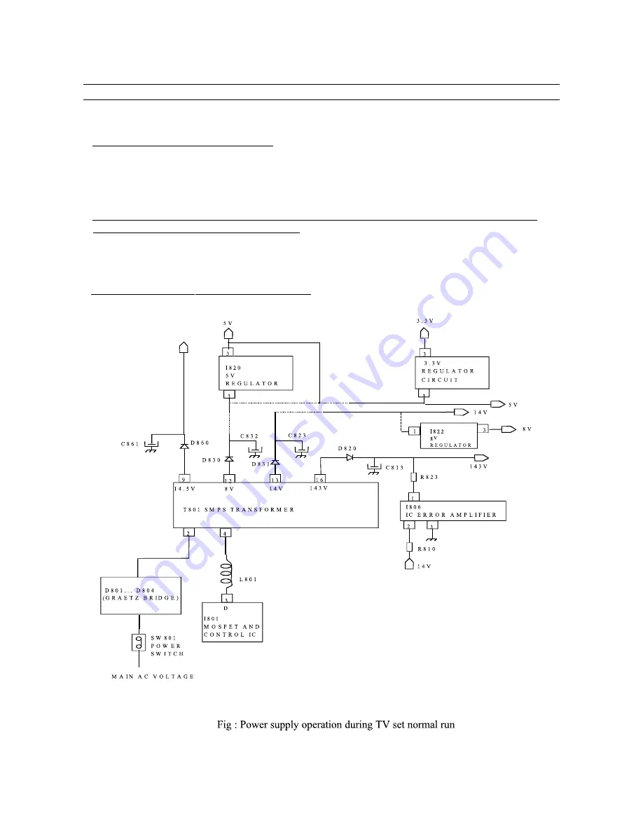
Therefore, the power circuit diagram is the following one :
* power supply circuit diagram during TV set normal run
Содержание CP-885
Страница 32: ... 31 Service manual WP 895 895F CP885 885F Block diagram TDA8944J ...
Страница 35: ... 34 Service manual WP 895 895F CP885 885F ...
Страница 37: ... 36 Service manual WP 895 895F CP885 885F Block diagram TDA6107Q ...
Страница 42: ... 41 Service manual WP 895 895F CP885 885F 5 Circuit description 5 1 Block diagram ...
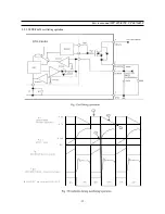
Страница 60: ... 59 Service manual WP 895 895F CP885 885F 5 9 2 2 STR F6654 oscillating operation ...
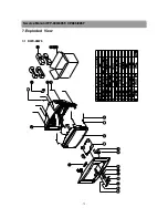
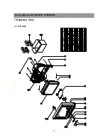
Страница 76: ...Service Manual WP 895 895F CP885 885F 75 7 Exploded View 7 1 DWX 28W5 ...
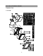
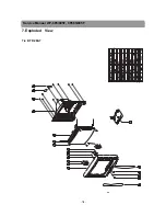
Страница 77: ...Service Manual WP 895 895F CP885 885F 76 7 Exploded View 7 2 DWF 28W8 ...
Страница 78: ...Service Manual WP 895 895F CP885 885F 77 7 Exploded View 7 3 DTF 29U8 ...
Страница 79: ...Service Manual WP 895 895F CP885 885F 78 7 Exploded View 7 4 DTP 28A7 ...
Страница 80: ...Service Man ual WP 895 895F CP885 885F 79 7 Exploded View 7 5 DTP 28B1 ...
Страница 81: ...Service Man ual WP 895 895F CP885 885F 80 7 Exploded View 7 6 DTP 28G7 ...
Страница 82: ...Service Manual WP 895 895F CP885 885F 81 7 Exploded View 7 7 DTP 28G8 ...
Страница 83: ...PRINTED CIRCUIT BOARD PCB MAIN ...
Страница 84: ......
Страница 85: ......

