background image

15

TROUBLE SHOOTING GUIDE

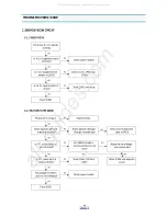
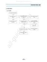
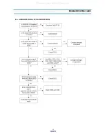
D. AUDIO CIRCUIT

D-1. PB MODE    

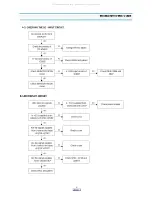
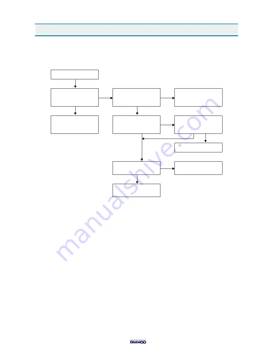
No sound in the PB mode

               YES

Is the output at pin77 of

  IC301?

NO

 Is +5V supplied to pin76 of

  IC301 and to pin2 of 

  T201?

NO

Check IC802 and adjacent

  circuit

               YES

               YES

Check R217, R218, L602

  and pattern

 Is voltage less than 0.2V

  at pin80 of IC301?

NO

Are CLK and DATA 

  applied to pin63 and 64 of

  IC301?

YES

               YES         NO

Check IC501

 Is collector of Q204 GND?

NO

 Check Q202, Q203 and

   Q204

               YES

Check pattern and AC 

   Head

All manuals and user guides at all-guides.com

all-guides.com

Содержание DV-S123W Series

Страница 1: ...LECTRONICS CO LTD URL http svc dwe co kr S M No VS123MUEF1 Multi Models S2 MECHA Caution In this Manual some parts can be changed for improving their performance without notice in the parts list So if...

Страница 2: ...IN ASSIGNMENT 29 PRINTED CIRCUIT BOARD 32 1 PCB MAIN 32 2 PCB POWER SMPS 33 CIRCUIT DIAGRAM 34 1 CONNECTION DIAGRAM 34 2 POWER CIRCUIT 35 3 SERVO SYSCON CIRCUIT 36 4 AV INPUT OUTPUT CIRCUIT 37 5 VIDEO...

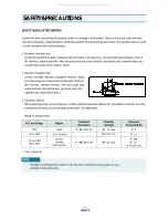
Страница 3: ...between power cord plug prongs and exposed accessible parts of the set RF terminals antenna terminals video and audio input output terminals microphone jack ear phone jacks etc is greater than values...

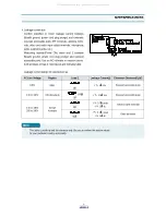
Страница 4: ...ltmeter to measure across both terminals of load Z See figure2 and following table Leakage current ratings for selected are as AC Line Voltage Region Load Z Leakage Current i Clearance Distance d d 10...

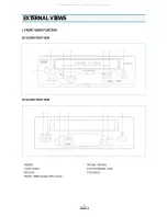
Страница 5: ...VIEWS 1 FRONT VIEWS FUNCTION DV S103W FRONT VIEW DV S123W FRONT VIEW POWER REVIND REVIEW STOP EJECT FAST FORWARD CUE RECORD PLAY BACK FRONT VIDEO AUDIO INPUT JACK All manuals and user guides at all g...

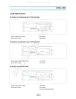
Страница 6: ...C12V INPUT JACK RE OUTPUT DV S103W DV S123W SCART JACK TYPE REAR VIEW EURO AUDIO VIDEO IN OUT JACK ANT INPUT DC12V INPUT JACK RF OUTPUT DV S103A DV S103N REAR VIEW AUDIO VIDEO IN OUT JACK ANT INPUT DC...

Страница 7: ...H1 2 Adjustment Adjust R591 to the positive rising edge of V SW PULSE at 6 5H 0 5H from the V SYNC 3 Adjustment Inspection Standard 6 5H 0 5H 4 REMARKS ITEM ADJUSTMENT PARTS CHECK POINT TEST EQUIPMENT...

Страница 8: ...CENELEC standard more than 47 unbalanced 6dBm CENELEC standard less than 1 unbalanced 100Hz 8KHz for PAL SP 100Hz 10KHz for NTSC SP More than 38dB for PAL SP More than 40dB for NTSC SP Less than 3 SP...

Страница 9: ...ondary circuit When changing M801 check FUSE and ceramic resistor properly A 1 CHECKING THE PRIMARY CIRCUIT A 2 CHECKING THE SECONDARDARY CIRCUIT Before secondary circuit open No output voltage YES Is...

Страница 10: ...06 and R807 YES Check SERVO SYSCON circuit LED does not operate properly NO Is 5 1V supplied from D510 cathod to L701 NO Check power module YES Is 5 1V supplied to the collectors of Q701 Q706 NO Check...

Страница 11: ...od NO Adjust tracking YES Noise appears although adjusting tracking NO Noise appears although Change cassette tape YES Check and re adiust the path of DECK YES Is CTL pulse output at pin1 of IC505 NO...

Страница 12: ...PG delay R591 YES YES YES NO Check R524 and pattern Check D PG input at pin13 of IC501 and P502 Is DC ENVE waveform input at pin39 of IC501 NO Is DC ENVE waveform output at pin6 of IC401 NO Check vid...

Страница 13: ...s 5V applied to pin6 of IC503 when CST IN NO Is control signal output at pin76 of IC501 NO Check IC501 YES YES Check pattern and R529 Is 8 2V supplied to pin4 of IC503 NO Are control signals output at...

Страница 14: ...of R555 R556 and R557 YES Is pin4 of P501 2 5V NO Check R559 and R560 YES Is C PWM output at pin34 of IC501 NO Check IC501 YES Check P501 R516 R526 and C526 Drum M T and capstan M T rotate at reular s...

Страница 15: ...ule YES Does X501 crysyal oscillate NO Check IC501 and crystal circuit YES Are CAM SW data cor rect NO Recheck P504 and CAM SW contact YES Check IC503 and IC501 VCP does not operate after power cord p...

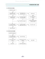
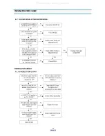
Страница 16: ...2 of T201 NO Check IC802 and adjacent circuit YES YES Check R217 R218 L602 and pattern Is voltage less than 0 2V at pin80 of IC301 NO Are CLK and DATA applied to pin63 and 64 of IC301 YES YES NO Check...

Страница 17: ...plied to pin63 and 64 of IC301 NO Check IC501 YES Is audio signal input into pin79 of IC301 NO Check C212 R215 R214 and C210 YES YES YES Does pin6 of T201 Oscillate NO Is the volatge from 0 7V to 3 0V...

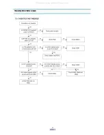
Страница 18: ...into pin71 of IC301 NO Check R609 R610 C218 and JK603 YES Is signal output at pin77 of IC301 NO Is 5V applied to pin76 and 47 of IC301 NO Check IC802 and adjacent circuit YES YES Check C212 R217 R218...

Страница 19: ...1 NO Is video signal input at pin30 of IC301 NO Check JK603 and pattern YES YES Check R312 Q604 and Adjacent circuit Are CLK DATA signals input at pin63 and 64 of IC301 NO Check SERVO SYSCON circuit a...

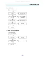
Страница 20: ...NO Check the ON OFF 5V YES Is REC H from pin79 of IC501 supplied to pin11 of IC401 at 0V NO Check Q503 Q504 and adjacent circuit YES Is V SW pulse from pin46 of IC501 supplied to pin4 of IC401 NO Chec...

Страница 21: ...d adjacent YES Is ON OFF 5V supplied to pin36 and 47 of IC301 NO Check the ON OFF 5V YES Is the luminance signal from pin15 fed to pin20 of IC301 through Q302 NO Check Q302 and adjacent Circuit YES Is...

Страница 22: ...1 NO Check the ON OFF 5V YES Is the colour signal from pin15 of IC301 fed to pin48 and 50 of IC301 NO Check IC301 YES Is the colour sinal from pin48 and 50 of IC301 fed to pin13 of IC302 NO Check C351...

Страница 23: ...from pin14 of IC301 fed to pin10 of IC401 NO Check C406 correct NO Changed damaged Components YES YES TO COLOUR SIGNAL IN THE REC MODE Is ON OFF 5V supplied to pin13 of IC401 at 5V NO Check ON OFF 5V...

Страница 24: ...O Change damaged Compoents YES YES Check IC301 Is the luminance signal from pin25 fed to pin26 of IC301 NO Are Q302 C312 C313 C342 R307 R308 R309 and R310 correct NO Changed damaged Components YES YES...

Страница 25: ...and adjacent circuit NO Changed damaged components YES YES TO PREAMP CIRCUIT IN THE REC MODE NO Check IC301 Check the output channel of VCP and input channel of TV NO Set the output channel of VCP re...

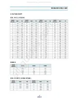
Страница 26: ...2 37 2 37 30 2 11 0 00 50 2 92 70 0 02 0 00 11 3 07 2 38 31 4 08 4 08 51 4 23 71 2 39 2 38 12 2 32 2 31 32 1 80 0 28 52 3 22 72 0 01 0 01 13 1 71 2 08 33 0 58 0 58 53 0 00 73 2 39 2 38 14 2 95 0 31 34...

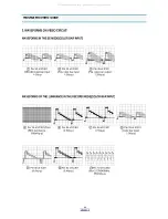
Страница 27: ...r input 1 0Vp p 2 Pin 30 of IC301 PAL color bar input 1 0Vp p 3 Pin 38 of IC301 PAL color bar output 2 0Vp p 4 Pin 18 of IC301 PAL REC luminance 300mVp p 6 Pin 25 of IC301 0 5Vp p 7 Pin 26 of IC301 0...

Страница 28: ...mVp p Pin 52 of IC301 400mVp p Pin 37 of IC301 C SYNC 2Vp p Pin 14 of IC301 300mVp p Pin 10 of IC401 REC PAL color 300mVp p 12 13 14 17 16 15 UP Pin 66 of IC301 color rotary 1Vp p DOWN Pin 20 of IC301...

Страница 29: ...APE UP Pin 66 of IC301 color rotary 0 5Vp p DOWN Pin 20 of IC301 500mVp p Pin 37 of IC301 Video out 2 0Vp p Pin 48 and 50 of IC301 240mVp p Pin 52 of IC301 300mVp p Pin 45 of IC301 500mVp p Pin 46 of...

Страница 30: ...P RF101 IC505 13 D_PG I DRUM PG INPUT P DECK DRUM 14 PWR ON L O POWER ON OFF CONTROL L POWER 15 REMOTE I REMOTE DATA INPUT P R_RECEIVER 16 CAP_I LIMIT O THIS PORT IS USUALLY OPEN BUT OUPUTS FOR FRAME...

Страница 31: ...C O OUPUT DURING TRICK MODE P L A V 48 C_ROT O INVERTED V_SW PULSE P A V 49 GRID_5 O LED GRID_5 OUTPUT P L DISPLAY 50 CAM_C I DECK CAM SW 51 CAM_B 52 CAM_A 53 REC_SAFETY L I REC SAFETY TAB IS DETECTED...

Страница 32: ...NT_5 OUTPUT P L DISPLAY 73 Vdd1 Vcc 74 A D RESET H O TO RESET AVref H 75 CAP_F R O CAP M T FORWARD L REVERSE H L H DECK CAP 76 LM_R O H L DECK LM M T IC503 77 LM_F O 78 CST IN L O TO OUTPUT L STATE IN...

Страница 33: ...32 PRINTED CIRCUIT BOARD 1 PCB MAIN All manuals and user guides at all guides com...

Страница 34: ...33 PRINTED CIRCUIT BOARD 2 PCB POWER SMPS All manuals and user guides at all guides com...

Страница 35: ...34 CIRCUIT DIAGRAM 1 CONNECTION DIAGRAM DV S103W S103A S103N All manuals and user guides at all guides com...

Страница 36: ...35 CIRCUIT DIAGRAM 2 POWER CIRCUIT DV S103W All manuals and user guides at all guides com a l l g u i d e s c o m...

Страница 37: ...36 CIRCUIT DIAGRAM 3 SERVO SYSCON CIRCUIT DV S103W All manuals and user guides at all guides com...

Страница 38: ...37 CIRCUIT DIAGRAM 4 AV INPUT OUTPUT CIRCUIT DV S103W All manuals and user guides at all guides com...

Страница 39: ...38 CIRCUIT DIAGRAM 5 VIDEO AUDIO CIRCUIT DV S103W S103A S103N S103S All manuals and user guides at all guides com...

Страница 40: ...39 EXPLODING VIEWS PARTS LIST 1 PACKING AS All manuals and user guides at all guides com...

Страница 41: ...40 EXPLODING VIEWS PARTS LIST 2 SET TOTAL ASSEMBLY All manuals and user guides at all guides com a l l g u i d e s c o m...

Страница 42: ...41 EXPLODING VIEWS PARTS LIST 3 FRONT PANEL ASSEMBLY DV S103W FRONT PANEL ASSEMBLY All manuals and user guides at all guides com...

Страница 43: ...42 EXPLODING VIEWS PARTS LIST DV S123W FRONT PANEL ASSEMBLY All manuals and user guides at all guides com...

Страница 44: ...AW063 PCB POWER AXIAL AS S103WY QB D A495600 D11 DZEG01C DIODE EG01C D12 DZEU01Z DIODE EU01Z JP01 85801060TA WIRE COPPER 0 6X52MM TAPING JP02 85801060TA WIRE COPPER 0 6X52MM TAPING R11 RD 4Z100JS R CA...

Страница 45: ...000PF K 2012 C515 HCBK103KCA C CHIP CERA 50V X7R 0 01MF K 2012 C516 HCBK102KCA C CHIP CERA 50V X7R 1000PF K 2012 C517 HCBK103KCA C CHIP CERA 50V X7R 0 01MF K 2012 LOC PART CODE PART NAME PART DESC C52...

Страница 46: ...FT103JCA R CHIP 1 10 10K OHM J 2012 R557 HRFT153JCA R CHIP 1 10 15K OHM J 2012 R558 HRFT103JCA R CHIP 1 10 10K OHM J 2012 R561 HRFT103JCA R CHIP 1 10 10K OHM J 2012 R567 HRFT102JCA R CHIP 1 10 1K OHM...

Страница 47: ...50V 0 022MF K AXL 52 C315 CCZB1H104K C CERA HIBK 50V 0 1MF K AXL 52MM C332 CCZB1H103K C CERA HIKB 50V 0 01MF K AXIAL C341 CBZP1C103M C CERA SEMI 16V Y5S 0 01MF M C351 CBZP1C103M C CERA SEMI 16V Y5S 0...

Страница 48: ...FILM 1 6 75K OHM J R578 RD AZ473J R CARBON FILM 1 6 47K OHM J LOC PART CODE PART NAME PART DESC R583 RD AZ103J R CARBON FILM 1 6 10K OHM J R584 RD AZ472J R CARBON FILM 1 6 4 7K OHM J R602 RD AZ750J R...

Страница 49: ...EGULATOR KA431AZ POWER L12 56X0000007 COIL BEAD BI 4865 5TS BASE POWER L21 56C220K695 COIL CHOKE CAP TYPE 22UH K CAP TYPE 9X11 1 POWER L22 56C220K686 COIL CHOKE 22UH K 27 5X0 4D POWER M801A 97PC316600...

Страница 50: ...80RD15 NTSC PAL 1 5M 97P880RN10 NTSC 1 0M D005 WARRANTY CARD 97P9407000 PAPER D006 ADAPTER 4859000240 2015A 300V D 4 0 03 CHASSIS MAIN AS PVMCASW063 S103WY QB D PC0204C S123W QB E S103A QB S103NY QD A...

Страница 51: ...CA 1 10 240 OHM J 2012 HRFT241JCA 1 10 240 OHM J 2012 R213 R CHIP HRFT682JCA 1 10 6 8K OHM J 2012 HRFT682JCA 1 10 6 8K OHM J 2012 HRFT223JCA 1 10 22K OHM J 2012 HRFT183JCA 1 10 18K OHM J 2012 R304 R C...

Страница 52: ...06 WIRE COPPER 85801065GY AWG22 1 0 65 TIN COATING JP107 WIRE COPPER 85801065GY AWG22 1 0 65 TIN COATING 85801065GY AWG22 1 0 65 TIN COATING JP108 WIRE COPPER 85801065GY AWG22 1 0 65 TIN COATING 85801...

Страница 53: ...AHYEON DONG MAPO GU SEOUL KOREA C P O BOX 8003 SEOUL KOREA TELEX DWELEC K28177 8 CABLE DAEWOOELEC E mail G7F00E web dwe co kr FAX 02 360 8184 TEL 02 360 8178 8187 PRINTED DATE FEB 1999 All manuals and...

Отзывы: