background image

CY3210-PSoCEVAL1 PSoC® 1 Evaluation Kit Guide, Doc. #: 001-66768 Rev. *F

47

Code Examples

Note

The measured value might have an error of upto 10 counts due to ADC offset or potentiom-

eter inaccuracy.

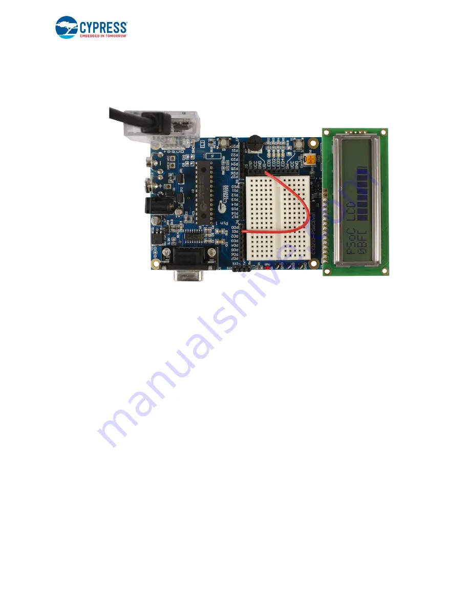
Figure 5-31.  LCD Displaying ADC Value

4. Vary the potentiometer and observe the change in the value of LCD.

Note

ADC values may fluctuate several counts due to system noise or if the potentiometer volt-

age is at the edge of an ADC count.

5. Save and close the project.

5.1.4

Verifying Output using UART

The PSoC project in 

“Creating My First PSoC 1 Project” on page 31

 uses an UART module in the

design. The ADC value that is displayed on the LCD can be viewed on a terminal application such as
HyperTerminal or TeraTerm on a PC. To view this output, apart from the hardware connections in

“Verifying Output using LCD” on page 46

, a RS-232 cable needs to be connected from the CY3210-

PSoCEVAL1 board to a COM port on a PC, as shown in 

Figure 5-32

.

Содержание PSoC 1 CY3210-PSoCEVAL1

Страница 1: ...CY3210 PSoCEVAL1 PSoC 1 Evaluation Kit Guide Doc 001 66768 Rev F Cypress Semiconductor 198 Champion Court San Jose CA 95134 1709 www cypress com...

Страница 2: ...ILITY AND FITNESS FOR A PARTICULAR PURPOSE To the extent permitted by applicable law Cypress reserves the right to make changes to this document without further notice Cypress does not assume any liab...

Страница 3: ...EVAL1 System Block Diagram 23 4 2 Functional Description 24 4 2 1 Power Supply System 24 4 2 2 Programming Interface 27 4 2 3 PSoC 1 Parts 27 4 2 4 RS 232 Interface 28 4 2 5 Prototyping Area 29 4 2 6...

Страница 4: ...60 5 5 Code Example 5 ASM_Example_Dynamic_PWM_PRS 61 5 5 1 Project Description 61 5 5 2 Hardware Connections 63 5 5 3 Code Example 5 Flowchart 64 5 5 4 Verifying Output 65 5 6 Code Example 6 ASM_Examp...

Страница 5: ...r and experience simpler and faster designs The evaluation board features a pluggable character LCD module with contrast control status LEDs a potentiometer push button switches a UART an RS 232 inter...

Страница 6: ...topics from basic to advanced level Recommended application notes for getting started with PSoC 1 are Getting Started with PSoC 1 AN75320 PSoC 1 Getting Started with GPIO AN2094 PSoC 1 Analog Structur...

Страница 7: ...dware settings 2 Parameters the parameters of the currently selected User Modules 3 Pinout information related to device pins 4 Chip Level Editor a diagram of the resources available on the selected c...

Страница 8: ...your design process by starting you off with a complete design instead of a blank page and also show how PSoC Designer User modules can be used for various applications http www cypress com go PSoC1Co...

Страница 9: ...heet for the selection on the Description tab Review the code example for the selection You can copy and paste code from this window to your project which can help speed up code development or Create...

Страница 10: ...evices User module datasheets Right click a User module and select Datasheet This datasheet explains the parameters and APIs of the selected user module Device Datasheet Choose Help Documentation Devi...

Страница 11: ...ntroductory project is included to help you develop PSoC 1 applications AN73212 Debugging with PSoC 1 This application note introduces the elements of the PSoC 1 debugger system and explains how to co...

Страница 12: ...plays file names and reference documentation Read about the sourcefile hex file in the PSoC Designer User Guide Bracketed Bold Displays keyboard commands in procedures Enter or Ctrl C File Open Repres...

Страница 13: ...download a CY3210 PSoCEval1_ISO This file ISO image is an archive file of the optical disc provided with the kit You can use this to create an installer DVD or extract information using WinRar or sim...

Страница 14: ...er 4 The InstallShield Wizard screen appears On this screen choose the folder location to install the setup files You can change the folder location for setup files using Change as shown in Figure 2 3...

Страница 15: ...n Type Options 8 When the installation begins a list of all packages appear on the Installation Page A green check mark appears against every package that is downloaded and installed as shown in Figur...

Страница 16: ...e After software installation drivers are installed when MiniProg1 is connected to the PC for the first time Verify driver installation by opening PSoC Programmer with the MiniProg connected to the US...

Страница 17: ...chapter on page 31 1 Click Start All Programs Cypress PSoC Designer version PSoC Designer ver sion Figure 2 7 PSoC Designer Interconnect View Note The Datasheet and Resource Meter windows are hidden...

Страница 18: ...grammer version PSoC Programmer version 2 Select the MiniProg from Port Selection Figure 2 8 PSoC Programmer Window 3 Click the File Load button to load the hex file 4 Use the Program button to progra...

Страница 19: ...lug in the MiniProg to the ISSP header Connect the MiniProg to the PC using the USB cable provided Power the kit using PSoC Programmer For more information on using PSoC Programmer see Programming Spe...

Страница 20: ...er six feet to avoid signal integrity issues When using MiniProg the LEDs blink at a variable rate to track connection status The green LED near the USB connector turns on after MiniProg is plugged in...

Страница 21: ...CY3210 PSoCEVAL1 PSoC 1 Evaluation Kit Guide Doc 001 66768 Rev F 21 Kit Operation Figure 3 2 Programming PSoC Device Figure 3 3 PSoC Programmer Screen...

Страница 22: ...DC_UART_LCD hex Click Open to select the hex file 6 Click Connect or double click on the respective MiniProg under Port Selection to select or con nect to MiniProg 7 Make sure the Power Cycle radio bu...

Страница 23: ...31 4 1 CY3210 PSoCEVAL1 System Block Diagram The CY3210 PSoCEVAL1 Evaluation Kit consists of Power supply system Programming interface PSoC 1 RS 232 interface Prototyping area Character LCD interface...

Страница 24: ...three ways using a MiniProg unit DC wall adaptor or a 9 V battery The DC wall adaptor must be of 9 V to 12 V 1 A rating unit The onboard voltage regulator converts input 9 V 12 V into 3 3 V 5 V Select...

Страница 25: ...tages applied at the external board connector Figure 4 4 is the protection circuit placed between the VCC domain near the prototype board on J5 connector and the onboard components This circuit discon...

Страница 26: ...nication and should be removed for normal I O operation JP2 connects P27 to Tx pin for UART communication and should be removed for normal I O operation JP3 controls the voltage regulator settings and...

Страница 27: ...corporate 12 bit ADC 6 bit DAC flexible internal clock generators 8 bit PWM and 8 bit counter Table 4 1 Pin Description Pin No Pin Name Description Connected To 1 P0 7 Analog column mux input J6 8 2 P...

Страница 28: ...ISSP SCLK J8 2 and XTALIN Sclk 14 VSS Ground connection Vss 15 P1 0 Crystal XTALout I2 C Serial Data SDA ISSP SDATA J8 1 and XTALout Sdata 16 P1 2 J8 3 17 P1 4 Optional external clock input EXTCLK J8...

Страница 29: ...nnections close to the prototyping area for convenience The area also has four LEDs and two push button switches for application evaluation including the Reset switch This area also includes a potenti...

Страница 30: ...hematic 4 2 6 Character LCD Interface The kit has a character 2 16 alphanumeric LCD module which goes into the character LCD header J9 The LCD runs on a 5 V supply and can function regardless of the v...

Страница 31: ...used at unity gain to supply the input to ADC UART This is an 8 bit universal asynchronous receiver transmitter UART The clock divider VC3 generates the baud clock for the UART by dividing 24 MHz by 1...

Страница 32: ...Code Examples Figure 5 1 New Project Window 5 To select the target device click Device Catalog as shown in Figure 5 2 Figure 5 2 Select Device Catalog 6 The Device Catalog window opens Select CY8C2946...

Страница 33: ...1 Evaluation Kit Guide Doc 001 66768 Rev F 33 Code Examples Figure 5 3 Device Catalog Window 7 In the Generate Main File Using option select C and click OK 8 By default the project opens in Chip view...

Страница 34: ...re the modules required for this design Also connect the modules together and to the pins on the PSoC In the User Modules section expand the ADCs folder Figure 5 5 User Modules Window 10 In this folde...

Страница 35: ...an integrator Switched Capacitor Type C is a filter and Type D is an integrator Refer to the ADCINC UM data sheet and Technical Reference Manual from Help Documentation for more details on analog blo...

Страница 36: ...In the User Modules window expand the Amplifiers folder and double click on PGA to place a programmable gain amplifier PGA in the design 14 By default the PGA is placed on the ACB00 analog block To c...

Страница 37: ...properties as shown in Figure 5 11 Figure 5 11 PGA User Module Properties 16 Click on AnalogColumn_InputSelect_1 multiplexer in the Design window and change the input multiplexer to AnalogColumn_Inpu...

Страница 38: ...roperties of the LCD UM Enable the BarGraph property to include additional APIs into the project and allow the bar graph display on the LCD Figure 5 13 LCD User Module Properties Notes a This UM does...

Страница 39: ...as shown in Figure 5 15 Figure 5 15 UART User Module Properties 19 Route the RX signal of UART to P1 6 There are two methods to do this a Auto Routing While holding the Shift key on the keyboard click...

Страница 40: ...Manual Routing Configure the look up table LUT on Row_0_Input2 to GlobalOddEven bus To do so click on the Row_0_Input_2 bus to open the Digital Interconnect window Figure 5 17 Digital InterConnect Wi...

Страница 41: ...dd_6 Select Port_1_6 from the drop down list in the Pin field click OK Figure 5 19 Pin Select Figure 5 20 Pin Select 22 Route the TX signal of UART to P2 7 There are two methods to do this a Auto Rout...

Страница 42: ...Figure 5 21 Auto Routing b Manual Routing Configure the LUT on Row_0_Output3 To do so click on Row_0_Output3 to open the Digital Interconnect window 23 In this window enable Row_0_Output_3_Drive_1 to...

Страница 43: ...oc 001 66768 Rev F 43 Code Examples 25 Click on GlobalOutEven_7 Select Port_2_7 from the drop down list in the Pin field click OK Figure 5 23 Pin Select Figure 5 24 Pin Select 26 Configure the Global...

Страница 44: ...es the baud clock for UART by dividing 24 MHz by 156 The UART internally divides UART clock VC3 in this example by 8 resulting in a baud rate of 19200 bits per second See the UART UM data sheet for de...

Страница 45: ...re 5 27 Connect MiniProg1 to Board The board can be programmed either through PSoC Designer IDE or by launching PSoC Pro grammer To program the board using PSoC Programmer see Programming Specificatio...

Страница 46: ...ollowing connections using the jumpers shunts and single strand jumper wires a Connect P01 to VR using a single strand jumper wire This connects one of the PSoC pins to the potentiometer b Place jumpe...

Страница 47: ...or if the potentiometer volt age is at the edge of an ADC count 5 Save and close the project 5 1 4 Verifying Output using UART The PSoC project in Creating My First PSoC 1 Project on page 31 uses an U...

Страница 48: ...Connected to RS 232 Cable 1 Connect the hardware as explained in Verifying Output using LCD on page 46 section 2 Open a terminal application such as HyperTerminal or TeraTerm with these parameters a...

Страница 49: ...Examples 3 Power the board by clicking on the Toggle Power button in the Program Part window 4 The ADC value is displayed on the HyperTerminal and on the LCD as shown in Figure 5 34 and Figure 5 35 Fi...

Страница 50: ...e ADC output hex values If the ADC has completed conver sion the output is displayed on the LCD as ASCII text The same is transmitted to the PC through a RS 232 cable 5 2 2 Creating the Project The pr...

Страница 51: ...es Figure 5 36 Device Configuration for ADC Conversion and LCD Display 5 2 3 Hardware Connections ADC input 0 Vdd Connect P01 to VR Serial Rx Place jumper shunt on JP1 to connect P16 and Rx Serial Tx...

Страница 52: ...52 Code Examples Figure 5 37 Hardware Connection Code Example 2 5 2 4 Code Example 2 Flowchart Start Initialize UART PGA ADC LCD Enable Global Interrupts Read Result Clear Flag Print Result to UART D...

Страница 53: ...value on the LCD The value displayed on the LCD should change as the potentiometer is turned see Figure 5 38 Note Remove jumper JP3 to verify output at 5 V The LCD display will not be seen at 3 3 V o...

Страница 54: ...CY3210 PSoCEVAL1 PSoC 1 Evaluation Kit Guide Doc 001 66768 Rev F 54 Code Examples Figure 5 40 Verify Output on HyperTerminal...

Страница 55: ...ect demonstrates how an LED blinks at a constant duty cycle using a hardware PWM PWM8 The clock dividers VC1 VC2 and VC3 are used to divide the 24 MHz system clock by 16 16 and 256 respectively The re...

Страница 56: ...it Guide Doc 001 66768 Rev F 56 Code Examples 5 3 2 Hardware Connections Connect P20 to LED1 Figure 5 42 Hardware Connection Code Example 3 5 3 3 Code Example 3 Flowchart Start PWM Enable PWM Interrup...

Страница 57: ...lowing user modules Counter8 An 8 bit counter is used to generate an interrupt at the DAC update rate 1 64 sine wave period By adjusting the counter period the DAC frequency and the resulting sine fre...

Страница 58: ...CY3210 PSoCEVAL1 PSoC 1 Evaluation Kit Guide Doc 001 66768 Rev F 58 Code Examples Figure 5 44 Device Configuration to Output a Sine Wave...

Страница 59: ...01 to VR DAC Output 0 Vdd Connect P05 to LED1 and CRO Figure 5 45 Hardware Connections Code Example 4 5 4 3 Code Example 4 Flowchart Start ADC Value Update Counter Turn on PGA Start DAC Read Data Clea...

Страница 60: ...d reset the board by pressing the RESET button or by power cycling the board LED1 is a sine wave output whose period is based on the ADC Turning the potentiometer changes the ADC value and controls th...

Страница 61: ...configurations The new configuration can be renamed based on the project All PSoC resources digital and analog blocks can be reused A loadable configuration can be deleted if no longer required Howev...

Страница 62: ...Config_ configname and LoadConfig_ configname are used to unload and load the required configurations Counter8 In the base configuration it takes a clock of 732 Hz as an input PRS8 The PRS configurati...

Страница 63: ...63 Code Examples Figure 5 49 PWM Configuration Figure 5 50 PRS Configuration 5 5 2 Hardware Connections User button Connect P14 to SW PWM pulse width or PRS pulse density Connect P20 to LED1 PWM term...

Страница 64: ...Hardware Connection Code Example 5 5 5 3 Code Example 5 Flowchart Start Clock Generator Load PRS Configuration Start PWM Unload PWM Configuration Load PRS Configuration Start PRS Load Compared Value...

Страница 65: ...he LCD module and power the board When the switch is released the PWM configuration is loaded and LED1 and LED2 blink with PWM Pulse Width and PWM Terminal Count respectively When the switch is presse...

Страница 66: ...signed to blink an LED using the output of two PWMs The outputs are combined using an AND gate in an output bus logic block This logical combination results in a beat frequency of 1 4 Hz PWM8 Two 8 bi...

Страница 67: ...de Example 6 5 6 3 Code Example 6 Flowchart 5 6 4 Verifying Output After the program is built and programmed into the device make all the hardware connections and reset the board by either pressing th...

Страница 68: ...Kit Guide Doc 001 66768 Rev F 68 Code Examples Figure 5 55 Verify Output Code Example 6 See Replace CY8C29466 24PXI with CY8C27443 24PXI on page 74 for instructions on how to replace the CY8C29466 24...

Страница 69: ...8 P20 20 P17 10 P16 18 P15 11 P14 17 P13 12 P12 16 Xin Sclk P11 13 Xout Sdata P10 15 SMP 9 Xres 19 Vcc 28 Vss 14 U2 0 1uF 16V C6 1 2 3 4 5 J11 VCC ISSP Connector P11A P10A TP4 DNP 330 R10 0 R15 D 1 3...

Страница 70: ...CY3210 PSoCEVAL1 PSoC 1 Evaluation Kit Guide Doc 001 66768 Rev F 70 Appendix A 2 Board Layout Figure A 1 Top Copper Layer...

Страница 71: ...CY3210 PSoCEVAL1 PSoC 1 Evaluation Kit Guide Doc 001 66768 Rev F 71 Appendix Figure A 2 Bottom Copper Layer...

Страница 72: ...CY3210 PSoCEVAL1 PSoC 1 Evaluation Kit Guide Doc 001 66768 Rev F 72 Appendix Figure A 3 Top Overlay...

Страница 73: ...D4 LED5 Red Red LED LUMEX SML LXT0805IW TR 19 5 R1 R2 R3 R4 R5 1K Resistor SMT PANASONIC ERJ6GEYJ102V 20 1 R6 10K Potentiometer Panasonic EVN D8AA03B14 21 1 R7 10K Potentiometer BOURNS 3352T 1 103LF 2...

Страница 74: ...extractor between the IC and the socket Gently pull the IC out evenly away from the board If an IC extractor is not available using a nonmetallic tool lift one side of the IC as shown in Figure A 4 Do...

Страница 75: ...CY3210 PSoCEVAL1 PSoC 1 Evaluation Kit Guide Doc 001 66768 Rev F 75 Appendix Figure A 6 Place New Chip...

Страница 76: ...3223525 04 11 2011 SASH Updated Code Examples chapter on page 31 Updated My First Code Example on page 31 Updated Project Description on page 31 Updated Figure 5 25 Figure 5 26 and Figure 5 29 C 3744...

Отзывы: