


enCoRe™ V CY7C643xx, enCoRe™ V LV CY7C604xx TRM, Document No. 001-32519 Rev *H
60
Analog-to-Digital Converter (ADC)
7.2
Brief Overview of ADC Components and Registers
This section provides an overview of the functions of the
ADC block and the application interface.
7.2.1
Interface Command/Status Block
The Interface command and status block provides the appli-
cation interface logic. This block has a state machine that is
used to generate the status and other relevant signals for all
instructions.
7.2.2
ADC
The ADC is a part of the temperature control block.
The ADC in enCoRe V can be connected to the Tempera-
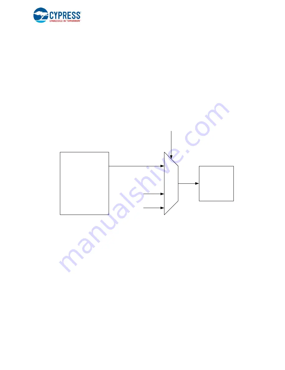
ture Sensor Core or the Analog Mux Bus as shown in
. As a default operation, the ADC is connected to
the temperature sensor to give digital values of the tempera-
ture.
Figure 7-2. Temperature Sensor/Analog Bus Connection to ADC
The ADC User Module contains an integrator block and one
comparator with positive and negative input set by the
MUXes. The input to the integrator stage comes from the
Analog Global Input Mux or the temperature sensor with full
scale input being 0V to 1.3V.
In the ADC only configuration (the ADC MUX selects the
Analog Mux Bus, not the default temperature sensor con-
nection), an external voltage can be connected to the input
of the modulator for voltage conversion. The ADC is run for
a number of cycles set by the timer, depending upon the
resolution of the ADC desired by the user. A counter counts
the number of trips by the comparator, which is proportional
to the input voltage. The Temp Sensor block clock speed is
36 MHz and is divided down to 1 to 12 MHz for ADC opera-
tion.
7.2.2.1 ADC Register Definitions on page 60
shows the reg-
isters that need to be configured for this conversion. A mini-
mum of 2
s wait time is required for the modulator to be
enabled after the other registers are configured. Therefore,
writes to the Modulator Control Registers (MOD_CR0 and
MOD_CR1) should be held for at least 2
s after all the
other registers are configured.
The registers specified below are controlled by the writing to
the interface commmand/status block.
7.2.2.1
ADC Register Definitions
The following registers (listed in table) are associated with
the ADC block in the temperature sensor core of enCoRe V
devices and are listed in address order. The register
descriptions have an associated register table showing the
bit structure for that register. The bits in the tables that are
grayed out are reserved bits and are not detailed in the reg-
ister descriptions that follow. Always write reserved bits with
a value of ‘0’.
Vbe
Vbe
Analog
Analog
ADC
MUX_SEL
TEMP
SENSOR
CORE
Vin
ADC


