


CapSense Technology
AN64846 - Getting Started with CapSense
®
Doc. No. 001-64846 Rev. *X
16
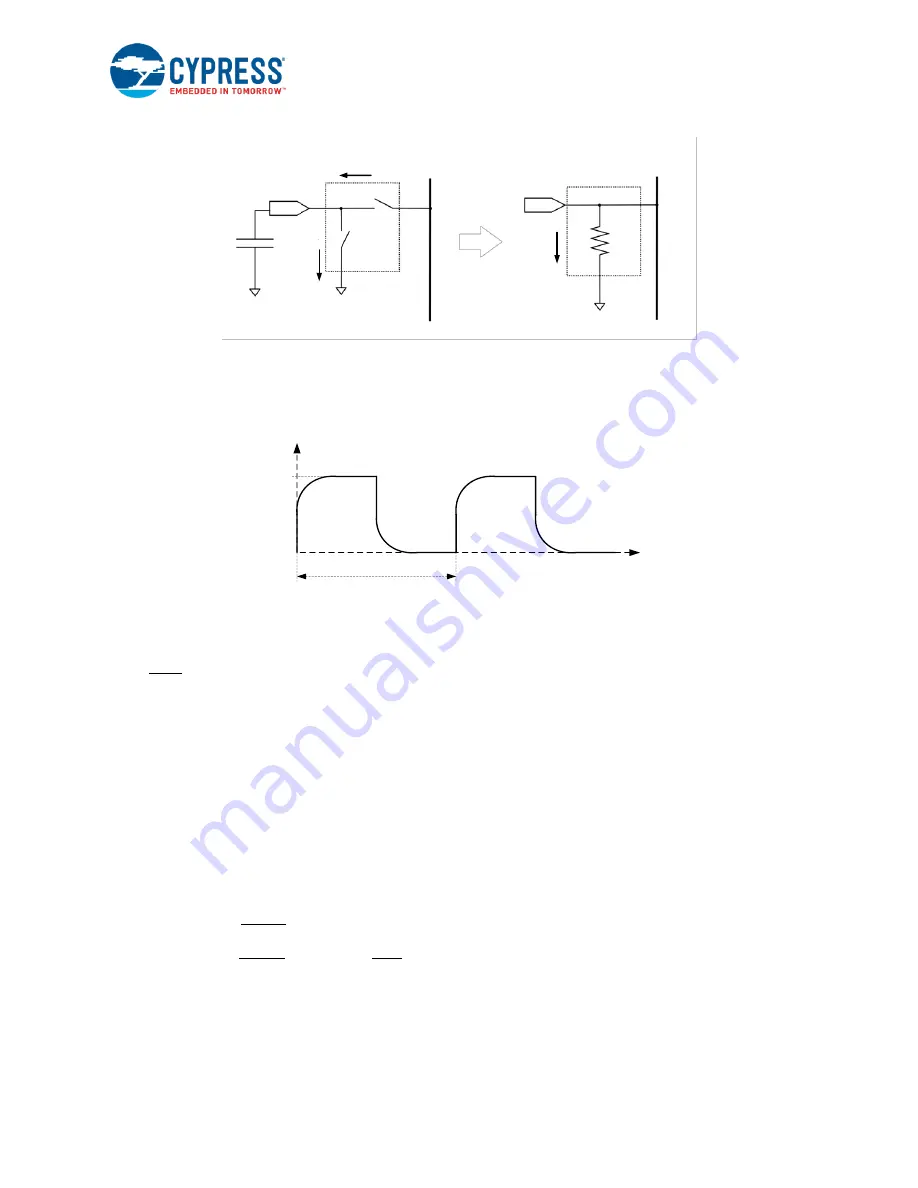
Figure 2-13. Equivalent Resistor Model
C
S
R
eq
AMUXBUS
SW
1
SW
2
AMUXBUS
I
CS
I
CS
I
CS
Two non-overlapping, out-of-phase clocks of frequency F
SW
(see
) control the switches SW
1
and SW
2
. F
SW
should be selected such that the sensor completely charges and discharges.
Figure 2-14. Voltage Across Sensor Capacitance
V
t
V
REF
(1.2V)
0
T
SW
= 1/F
SW
SW
1
OPEN
SW
2
CLOSED
SW
1
CLOSED
SW
2
OPEN
The continuous switching of SW
1
and SW
2
forms an equivalent resistance R
eq
, as
shows. The value of the
equivalent resistance R
S
is:
R
eq
=
1
C
S
F
SW
Equation 3
Where:
C
S
= Total sensor capacitance = Parasitic capacitance (C
P
) + Finger capacitance (C
F
)
F
SW
= Frequency of the switching clock or Sense Clock Frequency
Equation 4 gives the average current taken by the sensor capacitor from the AMUXBUS.
I
CS
= C
S
F
SW
V
REF
Equation 4
Equation 5 shows the raw count equation when only Modulation IDAC (single IDAC mode) is used and Equation 6
shows the raw count when both Modulation IDAC and Compensation IDAC (Dual IDAC mode) are used. The dual IDAC
mode gives more sensitivity and produces more count for a specific finger capacitance compared to the single IDAC
mode.
R
aw count = (2
N
− 1)
V
REF
F
SW
I
MOD
C
S
Equation 5
Raw count = (2
N
− 1)
V
REF
F
SW
I
MOD
C
S
− (2
N
− 1)
I
COMP
I
MOD
Equation 6
Where:
N = Scan resolution of the Sigma-Delta modulator in bits. CSD supports up to 16-bit resolution.
The CapSense architecture and its features vary slightly depending on the device. For example, some devices do not
support dual IDAC mode. The architecture presented here is available in many of the CapSense controllers. Refer to
the device-specific
to learn about the sensing technology implemented for that device.


