CY7C604XX
Document Number: 001-12395 Rev *H
Page 26 of 30
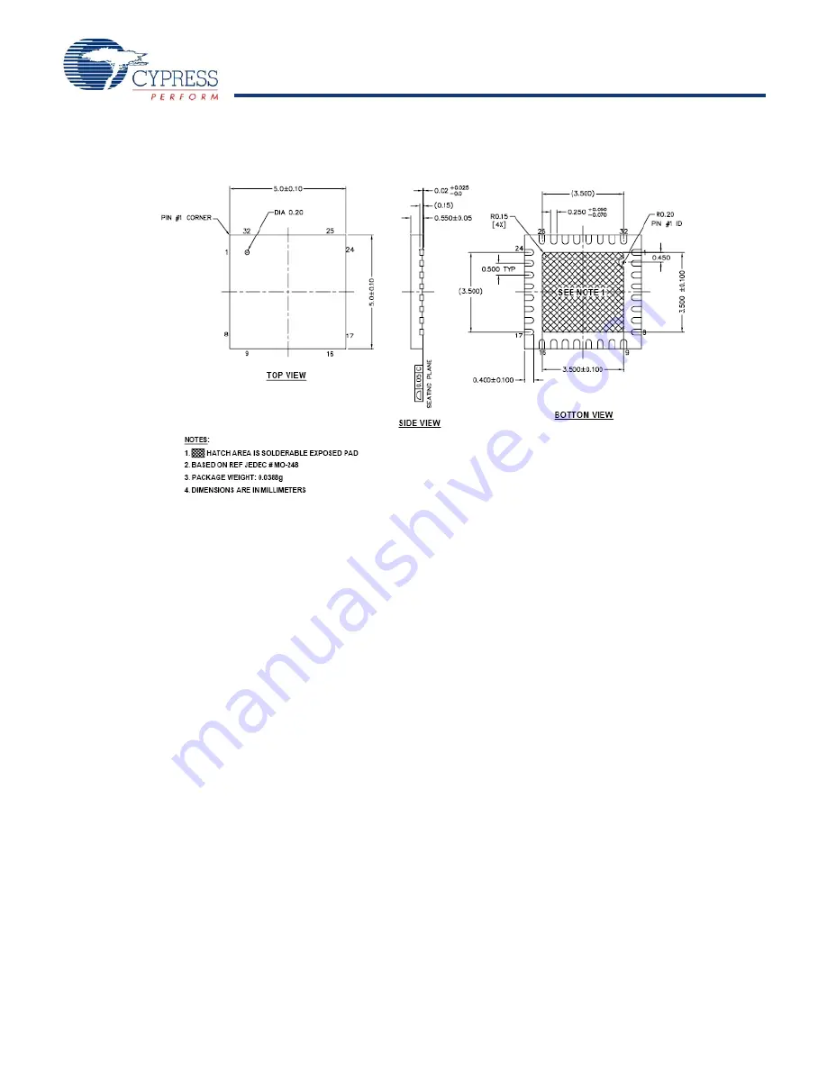
Figure 10. 32-Pin (5 x 5 x 0.55 mm) QFN (001-42168)
001-42168 *C
[+] Feedback
Страница 1: ...ical value Programmable Pin Configurations 25 mA sink current on all GPIO Pull Up High Z Open Drain CMOS drive modes on all GPIO Configurable inputs on all GPIO Low dropout voltage regulator for Port...
Страница 2: ...d for CPU intervention until a packet addressed to the target device has been received Low Voltage Detection LVD interrupts can signal the appli cation of falling voltage levels while the advanced POR...
Страница 3: ...e PSoC Designer interface and have been tested with a full range of debugging tools The choice is yours Assemblers The assemblers allow assembly code to be merged seamlessly with C code Link libraries...
Страница 4: ...r with valuator functions In the chip level view you perform the selection configuration and routing so that you have complete control over the use of all on chip resources Generate Verify and Debug W...
Страница 5: ...xample 14h or 3Ah Hexadecimal numbers may also be represented by a 0x prefix the C coding convention Binary numbers have an appended lowercase b for example 01010100b or 01000011b Numbers not indicate...
Страница 6: ...al I O I2C SDA SPI MISO 5 IOHR P1 3 Digital I O SPI CLK 6 IOHR P1 1 Digital I O ISSP CLK I2C SCL SPI MOSI 7 Power Vss Ground Pin 8 IOHR P1 0 Digital I O ISSP DATA I2C SDA SPI CLK 9 IOHR P1 2 Digital I...
Страница 7: ...SSP CLK I2C SCL SPI MOSI 12 Power Vss Ground connection 13 IOHR P1 0 3 4 Digital I O ISSP DATA I2C SDA SPI CLK 14 IOHR P1 2 Digital I O 15 IOHR P1 4 Digital I O optional external clock input EXTCLK 16...
Страница 8: ...I O 28 Power Vdd Supply voltage 29 IOH P0 7 Digital I O 30 IOH P0 5 Digital I O 31 IOH P0 3 Digital I O 32 Power Vss Ground connection CP Power Vss Center pad must be connected to ground LEGEND I Inp...
Страница 9: ...3 3 Digital I O 11 I O P3 1 Digital I O 12 IOHR P1 7 Digital I O I2C SCL SPI SS 13 IOHR P1 5 Digital I O I2C SDA SPI MISO 14 NC NC No connection 15 NC NC No connection 16 IOHR P1 3 Digital I O SPI CLK...
Страница 10: ...O 30 I O P3 6 Digital I O 31 I O P4 0 Digital I O 32 I O P4 2 Digital I O 33 I O P2 0 Digital I O 34 I O P2 2 Digital I O 35 I O P2 4 Digital I O 36 I O P2 6 Digital I O 37 IOH P0 0 Digital I O 38 IOH...
Страница 11: ...total register address space of 512 bytes The register space is also referred to as IO space and is broken into two parts Bank 0 user space and Bank 1 config uration space The XIO bit in the Flag reg...
Страница 12: ...2C_CFG D6 RW 17 57 97 I2C_SCR D7 18 58 98 I2C_DR D8 RW 19 59 99 D9 1A 5A 9A INT_CLR0 DA RW 1B 5B 9B INT_CLR1 DB RW 1C 5C 9C INT_CLR2 DC RW 1D 5D 9D INT_CLR3 DD RW 1E 5E 9E INT_MSK2 DE RW 1F 5F 9F INT_...
Страница 13: ...16 56 96 D6 17 57 97 D7 18 58 98 D8 19 59 99 D9 1A 5A 9A DA 1B 5B 9B DB 1C 5C 9C IO_CFG DC RW 1D 5D 9D OUT_P1 DD RW 1E 5E 9E DE 1F 5F 9F DF 20 60 A0 OSC_CR0 E0 RW 21 61 A1 ECO_CFG E1 22 62 A2 OSC_CR2...
Страница 14: ...ltage 1 71V 3 MHz V a l i d O p e r a t i n g R e g i o n 3 6V 750 kHz 6 MHz 24 MHz IMO Frequency Vdd Voltage 3 MHz 1 71V SLIMO Mode 01 12 MHz SLIMO Mode 00 SLIMO Mode 10 Table 7 Units of Measure Symb...
Страница 15: ...curacy DNL 1 2 LSb For any configuration INL 2 2 LSb For any configuration Offset Error 0 15 90 mV Operating Current 275 350 A Data Clock 2 25 12 MHz Source is chip s internal main oscillator See AC C...
Страница 16: ...d storage temperature is 25 C 25 C Extended duration storage temperatures above 85 C degrade reliability 6 Human Body Model ESD 7 According to JESD78 standard 8 The temperature rise from ambient to ju...
Страница 17: ...d for 3V Out IOH 10 A Vdd 3 1V maximum of 4 I Os all sourcing 5 mA 2 85 3 00 3 3 V VOH6 High Output Voltage Port 1 Pins with LDO Regulator Enabled for 3V Out IOH 5 mA Vdd 3 1V maximum of 20 mA source...
Страница 18: ...LDO Regulator Disabled for Port 1 IOH 2 mA maximum of 10 mA source current in all I Os Vdd 0 5 V VOH5A High Output Voltage Port 1 Pins with LDO Enabled for 1 8V Out IOH 10 A Vdd 2 4V maximum of 20 mA...
Страница 19: ...ulator Disabled for Port 1 IOH 100 A maximum of 10 mA source current in all I Os Vdd 0 2 V VOH4 High Output Voltage Port 0 or 1 Pins with LDO Regulator Disabled for Port 1 IOH 2 mA maximum of 10 mA so...
Страница 20: ...71 V IDDP Supply Current During Programming or Verify 5 25 mA VILP Input Low Voltage During Programming or Verify VIL V VIHP Input High Voltage During Programming or Verify VIH V IILP Input Current wh...
Страница 21: ...IMO 40 50 60 TRAMP Supply Ramp Time 0 s Table 16 AC GPIO Specifications Symbol Description Conditions Min Typ Max Units FGPIO GPIO Operating Frequency Normal Strong Mode Port 0 1 0 0 6 MHz for 1 71V V...
Страница 22: ...equency 0 750 25 2 MHz High Period 20 6 5300 ns Low Period 20 6 ns Power Up IMO to Switch 150 s TFall TRise23 TRise01 90 10 GPIO Pin Output Voltage Table 18 AC Programming Specifications Symbol Descri...
Страница 23: ...ifications Symbol Description Min Typ Max Units FSPIM Maximum Input Clock Frequency Selection Master 21 2 4V Vdd 3 6V 12 MHz Maximum Input Clock Frequency Selection Master 21 1 71V Vdd 2 4V 6 FSPIS Ma...
Страница 24: ...START Condition 4 7 0 6 s THDDATI2C Data Hold Time 0 0 s TSUDATI2C Data Setup Time 250 100 22 ns TSUSTOI2C Setup Time for STOP Condition 4 0 0 6 s TBUFI2C Bus Free Time Between a STOP and START Condit...
Страница 25: ...ice along with the thermal impedances for each package Important Note Emulation tools may require a larger area on the target PCB than the chip s footprint For a detailed description of the enCoRe V L...
Страница 26: ...CY7C604XX Document Number 001 12395 Rev H Page 26 of 30 Figure 10 32 Pin 5 x 5 x 0 55 mm QFN 001 42168 001 42168 C Feedback...
Страница 27: ...label on the package has details about the actual bake temperature and the minimum bake time to remove this moisture The maximum bake time is the aggregate time that the parts exposed to the bake tem...
Страница 28: ...C 32 Pin QFN 5x5x0 55 mm 16K 1K 28 Feature Rich Wireless Mouse CY7C60445 32LQXCT 32 Pin QFN Tape and Reel 5x5x0 55 mm 16K 1K 28 Feature Rich Wireless Mouse CY7C60455 48LTXC 48 Pin QFN 7x7x0 9 mm 16K 1...
Страница 29: ...Code table Ordering code changed for 32 QFN package From 32LKXC to 32LTXC Added a new package type LTXC for 48 QFN Included Tape and Reel ordering code for 32 QFN and 48 QFN packages Changed active cu...
Страница 30: ...nt Any reproduction modification translation compilation or representation of this Source Code except as specified above is prohibited without the express written permission of Cypress Disclaimer CYPR...