CY7C1019D
Document #: 38-05464 Rev. *E
Page 9 of 11
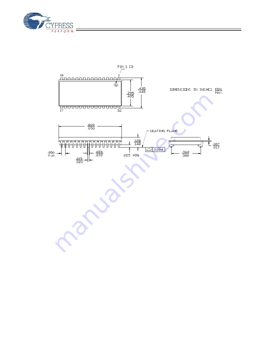
Package Diagrams
Figure 1. 32-pin (400-Mil) Molded SOJ (51-85033)
51-85033-*B
[+] Feedback
Страница 1: ...wer down feature that significantly reduces power consumption when deselected The eight input and output pins IO0 through IO7 are placed in a high impedance state when Deselected CE HIGH Outputs are disabled OE HIGH When the write operation is active CE LOW and WE LOW Write to the device by taking Chip Enable CE and Write Enable WE inputs LOW Data on the eight IO pins IO0 through IO7 is then writt...
Страница 2: ...ss Time 10 ns Maximum Operating Current 80 mA Maximum Standby Current 3 mA Top View SOJ TSOPII 1 2 3 4 5 6 7 8 9 10 11 14 19 20 24 23 22 21 25 28 27 26 12 13 29 32 31 30 16 15 17 18 A7 A1 A2 A3 CE IO 0 IO 1 VCC A13 A16 A15 OE IO 7 IO 6 A12 A11 A10 A9 IO 2 A0 A4 A5 A6 IO 4 VCC IO 5 A8 IO 3 WE VSS A14 VSS Feedback ...
Страница 3: ...to 85 C 5V 0 5V 10 ns Electrical Characteristics Over the Operating Range Parameter Description Test Conditions 10 Industrial Unit Min Max VOH Output HIGH Voltage IOH 4 0 mA 2 4 V VOL Output LOW Voltage IOL 8 0 mA 0 4 V VIH Input HIGH Voltage 2 2 VCC 0 5 V VIL Input LOW Voltage 2 0 5 0 8 V IIX Input Leakage Current GND VI VCC 1 1 µA IOZ Output Leakage Current GND VI VCC Output Disabled 1 1 µA ICC ...
Страница 4: ...hermal Resistance Junction to Case 38 14 21 43 C W AC Test Loads and Waveforms 4 90 10 3 0V GND 90 10 ALL INPUT PULSES CAPACITIVE LOAD CONSISTS OF ALL COMPONENTS OF THE TEST ENVIRONMENT Rise Time 3 ns Fall Time 3 ns 30 pF OUTPUT Z 50Ω 50 Ω 1 5V b a 5V OUTPUT 5 pF c R1 480Ω R2 255Ω High Z characteristics INCLUDING JIG AND SCOPE Notes 3 Tested initially and after any design or process changes that m...
Страница 5: ...l transition time of 3 ns or less timing reference levels of 1 5V input pulse levels of 0 to 3 0V and output loading of the specified IOL IOH and 30 pF load capacitance 6 tPOWER gives the minimum amount of time that the power supply should be at typical VCC values until the first memory access can be performed 7 tHZOE tHZCE and tHZWE are specified with a load capacitance of 5 pF as in c of AC Test...
Страница 6: ...ad Cycle No 1 Address Transition Controlled 13 14 Read Cycle No 2 OE Controlled 14 15 4 5V 4 5V tCDR VDR 2V DATA RETENTION MODE tR CE VCC PREVIOUS DATA VALID DATA VALID RC tAA tOHA tRC ADDRESS DATA OUT 50 50 DATA VALID tRC tACE tDOE tLZOE tLZCE tPU HIGH IMPEDANCE tHZOE tHZCE tPD HIGH ICC ISB IMPEDANCE OE CE ADDRESS DATA OUT VCC SUPPLY CURRENT Notes 12 Full device operation requires linear VCC ramp...
Страница 7: ...tAW tSA tPWE tHA tHD tSD tSCE tSCE CE WE DATA IO ADDRESS tHD tSD tPWE tSA tHA tAW tSCE tWC tHZOE DATAIN VALID NOTE 18 CE ADDRESS WE DATA IO OE Notes 16 Data IO is high impedance if OE VIH 17 If CE goes HIGH simultaneously with WE going HIGH the output remains in a high impedance state 18 During this period the IOs are in the output state and input signals should not be applied Feedback ...
Страница 8: ...tputs Disabled Active ICC Ordering Information Speed ns Ordering Code Package Diagram Package Type Operating Range 10 CY7C1019D 10VXI 51 85033 32 pin 400 Mil Molded SOJ Pb free Industrial CY7C1019D 10ZSXI 51 85095 32 pin TSOP Type II Pb free Please contact your local Cypress sales representative for availability of these parts Switching Waveforms continued DATA VALID tHD tSD tLZWE tPWE tSA tHA tAW...
Страница 9: ...CY7C1019D Document 38 05464 Rev E Page 9 of 11 Package Diagrams Figure 1 32 pin 400 Mil Molded SOJ 51 85033 51 85033 B Feedback ...
Страница 10: ... safety applications unless pursuant to an express written agreement with Cypress Furthermore Cypress does not authorize its products for use as critical components in life support systems where a malfunction or failure may reasonably be expected to result in significant injury to the user The inclusion of Cypress products in life support systems application implies that the manufacturer assumes a...
Страница 11: ... Switching Characteristics table Added Data Retention Characteristics table and waveforms Shaded Ordering Information C 307598 See ECN RKF Reduced Speed bins to 10 and 12 ns D 520647 See ECN VKN Converted from Preliminary to Final Removed Commercial Operating range Removed 12 ns speed bin Added ICC values for the frequencies 83MHz 66MHz and 40MHz Updated Thermal Resistance table Updated Ordering I...