background image

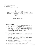
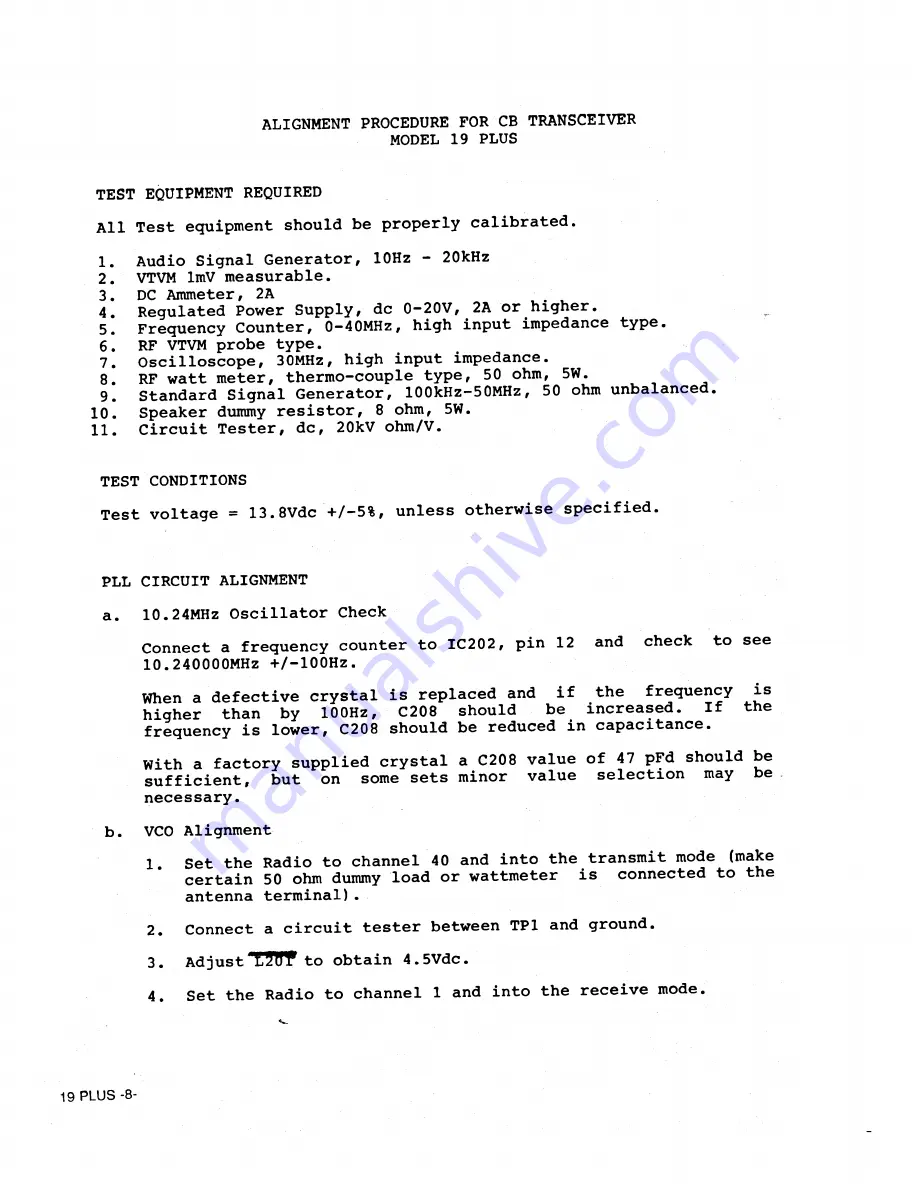
ALIGNMENT  PROCEDURE  FOR CB TRANSCEIVER


MODEL  19  PLUS

TEST EQUIPMENT REQUIRED

All Test  equipment  should be  properly  calibrated.

1. 

Audio  Signal  Generator,  10Hz  -  20kHz

2. 

VTVM  1mV measurable.

3. 

DC Ammeter,  2A 

.

4. 

Regulated Power  Supply,  de  0-20V,  2A or higher,

5. 

Frequency Counter,  0-40MHz,  high  input  impédance  type.

6. 

RF VTVM probe  type.

7. 

Oscilloscope,  30MHz,  high  input  impédance.

8. 

RF watt meter,  thermo-couple  type,  50  ohm,  5W.

9. 

Standard  Signal  Generator,  100kHz-50MHz,  50  ohm unbalanced.

10. 

Speaker  dummy  resistor,  8  ohm,  5W.

11. 

Circuit Tester,  de,  20kV ohm/V.

TEST CONDITIONS

Test voltage =  13.8Vdc  +/-5%,  unless  otherwise  specified.

PLL CIRCUIT ALIGNMENT

a. 

10.24MHz  Oscillator Check

Connect  a  frequency  counter  to  IC202,  pin  12  and  check  to  see


10.240000MHz  +/-100HZ.

When  a defective  crystal  is  replaced  and  if  the  frequency  is


higher  than  by 

100Hz, 

C208 

should 

be  increased. 

If  the


frequency  is  lower,  C208  should be  reduced  in capacitance.

With  a  factory  supplied  crystal  a C208  value of  47  pFd  should be


sufficient, 

but  on  some  sets minor  value  sélection  may  be


necessary.

b. 

VCO Alignment

1. 

Set  the  Radio  to  channel  40  and  into  the  transmit mode  (make


’ 

certain  50  ohm dummy  load  or Wattmeter  is  connected  to the

antenna  terminal).

2. 

Connect  a  circuit  tester between TPI  and ground.

3. 

Adjust 1 2 W  to obtain  4.5Vdc.

4. 

Set  the  Radio  to channel  1  and  into  the  receive mode.

19  PLUS  -8-

Содержание 19 Plus

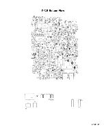
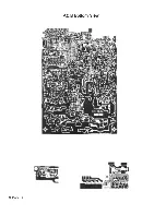
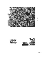
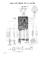
Страница 1: ...1261 B TOP VIEW 14 PARTS LAYOUT PCB401068 F BOTTOM VIEW 15 PARTS LAYOUT PCB 401377 C 401261 B BOTTOM VIEW 15 COMPOSITE LAYOUT PCB401068 F BOTTOM VIEW 16 COMPOSITE LAYOUT PCB 401377 C 401261 B BOTTOM VIEW 16 COPPER PATTERN PCB401068 F BOTTOM VIEW 17 COPPER PATTERN PCB 401377 C 401261 B BOTTOM VIEW 17 WIRING DIAGRAM CHASSIS MIC PINS 18 PCB 401068 D WIRING DIAGRAM 19 SEMICONDUCTOR PIN CONFIGURATION 2...

Страница 2: ...of reference oscillator VCO phase comparator and DC filter Iow pass filter With the above circuit the VCO Voltage Controlled Oscillator frequency is effectively locked to the reference oscillator and its accuracy is as good as the reference oscillator Since the CB radio s adjacent channel spacing is 10 kHz or multiple of 5 kHz our purpose should be to produce multiples of programable frequencies t...

Страница 3: ... mixed again with 10 24MHz crystal oscillator frequency which serves as the second local oscillator 10 695 10 24 0 455MHz As can be seen above the VCO frequency shifts from 16 725 to 16 27MHz when changed from transmit to receive for the same channel 1 The shift is accomplished by read only memory incorporated inside the PLL IC 202 between the selector switch and the VCO divider programable When t...

Страница 4: ...amplifier switch circuit When VCO frequency is out of LOCK condition pin 14 of IC202 pulls down bias voltage of Q301 to ground disabling Q301 from passing possible illegal frequencies Q302 is a RF power driver circuit and Q303 is the final RF power amplifier A modulation audio signal is applied to the collectors of Q302 and Q303 through an audio power transformer T501 The audio signal mic input is...

Страница 5: ...duces audio signal as well as a negative DC voltage for AGC action The negative voltage also provides forward biasing to the cathode of ANL clipping diode of D106 The biasing voltage has a time constance determined by RI24 and C123 Therefore any sharp negative going pulse from D103 will back bias D106 and be clipped 4 Channel Up Down Operation The PLL TX RX frequency channel number display channel...

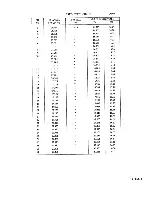
Страница 6: ...16 44 16 27 155 99 16 915 16 46 17 26 165 99 16 925 16 47 18 27 175 99 16 935 16 48 19 27 185 99 16 945 16 49 20 27 205 99 16 965 16 51 21 27 215 99 16 975 16 52 22 27 225 99 16 985 16 53 23 27 255 99 17 015 16 56 24 27 235 99 16 995 16 54 25 27 245 99 17 005 1 6 55 26 27 265 99 17 025 16 57 27 27 275 99 17 035 16 58 28 27 285 99 17 045 16 59 29 27 295 99 17 055 16 60 30 27 305 99 17 065 16 61 31 ...

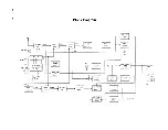
Страница 7: ...19 PLUS 6 Block Diagram ...

Страница 8: ... z smd 61 T X 26 PLL Circuit Block Diagram ...

Страница 9: ... 8Vdc 5 unless otherwise specified PLL CIRCUIT ALIGNMENT a 10 24MHz Oscillator Check Connect a frequency counter to IC202 pin 12 and check to see 10 240000MHz 100HZ When a defective crystal is replaced and if the frequency is higher than by 100Hz C208 should be increased If the frequency is lower C208 should be reduced in capacitance With a factory supplied crystal a C208 value of 47 pFd should be...

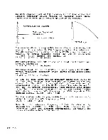
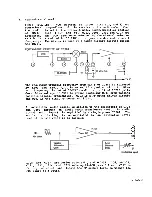
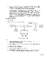
Страница 10: ... the lower value drops only to 1 5Vdc then a C216 of 82 pFd should be reduced toincrease the range This should not be necessary when factory supplied parts are used for D208 Varactor Diode and L201 VCO Tuning Coil TRANSMITTER ALIGNMENT a Test Set up Volt Ornent Meter Meter Note Transmitter Alignment Set Up 1 When connecting audio cable to the microphone input circuit always use shielded cable 2 Wh...

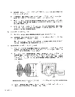
Страница 11: ... no modulation 2 Connect the frequency counter to the antenna load or to the tab provided at the watt meter The frequency should be within 800HZ from each channel center frequency as tabulated in Table 1 d Modulation Sensitivity Alignment 1 Set the unit to transmit mode of operation Feed 1kHz 30mV signal to the microphone input circuit and adjust RV501 so that 100 modulation is obtained 2 To set t...

Страница 12: ... alignment due to AGC action c Squelch Circuit Alignment 1 Set a 50 ohm signal generator to generate a signal on channel 19 with an output level of 1000 microvolts modulated 30f with a 1kHz tone 2 Rotate the squelch control in füll clockwise direction 3 Temporarily adjust RV101 for maximum audio output and note the audio output level Then adjust RV101 so that the audio output level decrèases by 6d...

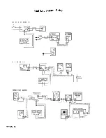
Страница 13: ...Test Equipment Setup PLL AND CARRIER SECTION P T T RECEIVER SECTION TRANSMITTER SECTION 19 PLUS 12 ...

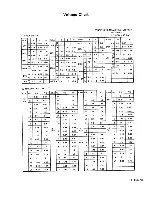
Страница 14: ...87 п а п а RX 0 4 2 0 7 8 0 0 Ю 6 SO H 0 7 0 0 0 3 0 2 RX 0 0 13 5 TX 0 4 0 0 7 7 9 2 INTEGRATED CIRCUIT IC N0 PIN RX TX IC N0 PIN RX TX IC N0 PIN RX TX IC NO 1 PIN RX TX 1 0 21 0 21 21 0 0 13 0 0 IC 1 0 0 IC 201 2 0 21 0 22 22 0 0 14 1 45 4 10 401 2 10 81 0 0 6 3 2 38 0 41 23 0 0 15 1 74 1 60 3 11 45 0 0 6 4 6 0 5 93 24 0 6 7 7 81 16 1 74 1 61 4 10 75 0 07 5 2 0 2 05 25 3 08 3 11 17 1 37 3 06 5 1...

Страница 15: ...ß CÛ 19 PLUS 14 ...

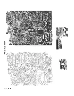
Страница 16: ...o 5 4 _VW_R4I2 AW 413 T C40I 4 Oq o o Л Л 3ÏXs o m Ю I A _SJ32 О С 1Я Ч feJSŁ S ReôT Htè S J 2 0 SJ30 SJI9_ JD 7 C203 sjie Omj a O Л _ I tV 3îQ ut f И У T CFI flN ourl I Æ jS L 0э г R 3 0 6 L b 3 cso eH I Q T xL yl ü ü s QSiOlJP P 7 CI34 I I f e u r C32I 2 g i T s EXT H O O O O O S 4 J I JR 19 PLUS 15 ...

Страница 17: ...P C B Bottom View 19 PLUS 16 ...

Страница 18: ...401377 с 19 PLUS 17 40I06S ...

Страница 19: ...Wiring Diagram Chassis and Microphone Pins ANT POWER JACK S P E A K E R VOLUME POWER ON OFF SW MIC DIN JACK SQUELCH GRN 0 5 4 0 5 19 PLUS 18 ...

Страница 20: ...BRN 3 1 6 3 P C B Wiring Diagram t o I ш i r o O BRN 3 1 3 3 ORG 3 1 6 3 19 PLUS 19 GRN 3 I 3 3 ...

Страница 21: ... LC7I3I LM64I6E TL489C P fi MC78L08CT output gnd mput TRANSISTORS MPS94I8 MPS 9623 MPS963I MPS 9681 MPS 9634 M PS9426 Ec 2SC23I4 DIODES IN 4002 IS 2473 OA 90 U Z P 8 2 B B ZX83 C 5V6 ł MV2209 ł SLB55VR3 L T D 4 8 2 6 Y LD OOIVR 19 PLUS 20 ...

Страница 22: ...OP DATA POINTER C CARRY FF PC PROGRAM COUNTER P D O 3 PA O 3 INT RËS XTAL O EXTAL O VOD O VSS LC 7131 I 2 3 4 5 6 8 9 16 TA 73I0P 19 PLUS 21 ...

Страница 23: ...BOOT STRAP D C DECOUPLING P C PHASE COMPENSATION T L 4 8 9 CP GND Ql 02 0 3 DIGITAL OUTPUTS 19 PLUS 22 ...

Страница 24: ...78 29 760430 Heat Sink TR MTG 30 504203 3P Plug Ass y 31 730477 Holder ANT MTG 32 992440 Ant Receptacle W Nut Washer 33 793100 Name Plate 34 670025 Rivet Blind 35 770830 Shield Plate 36 715540 Bottom Cover 37 900133 Feit 38 901767 Feit Strip BLK 39 4201030 Speaker 40 730015 Holder Speaker 41 720050 Bracket Mic MTG 42 715550 Upper Cover 43 720916 Bracket Set MTG 44 600051 Securing Screw 45 660138 W...

Страница 25: ...Exploded View 19 PLUS 24 ...

Страница 26: ...S ch em a tic Diagram 19 PLUS 25 ...

Страница 27: ...5 01 010 773 126 9 001 RFC201 INDUCTOR 25дН MOLD TYPE 047 049 9 001 J11 15 FLAT WIRE 5 PIN 40MM 428 130 9 001 RFC203 INDUCTOR 0 45дН MOLD TYPE 047 049 9 002 SLIDE SW KSA 2251T 2P 2C 084 160 9 001 RFC102 204 COIL CHOKE ЮОдН MO TYPE 047 027 9 001 SW1 2 TACK SWITCH KHG10905 088 155 9 001 RFC202 COIL CHOKE 4дН BOBBIN TYPE 047 012 9 004 RES VARIABLE VR L601 INDUCTOR 6 8дН MOLDED TYPE 047 050 9 001 VR10...

Отзывы: