background image

Introduction

Specifications 1 - 3

1.Introduction

Interface

One USB 2.0 Port

One USB 3.0 (USB 3.1 Gen 1) Type-A Port 

One USB 3.1 Gen 2 Type-A Port 

One USB 3.1 Gen 2 Type-C Port*

One HDMI-Out Port

Two Mini DisplayPorts

One External Monitor Port

One Headphone-Out Jack

One Microphone-In Jack

One RJ-45 LAN Jack

One DC-in Jack

Card Reader

Embedded Multi-In-1 Card Reader 

MMC (MultiMedia Card) / RS MMC

SD (Secure Digital) / Mini SD / SDHC/ SDXC

M.2 Slots

Slot 1 for 

Combo WLAN and Bluetooth

 Module

Slot 2 for 

SATA

 or 

PCIe Gen3 x4


SSD

USB 3.1 Gen 2

Note that when a single USB device is 
plugged in to a USB 3.1 Gen 2 port the data 
transfer speed will be 10Gbps, however when 
two devices are plugged in to both USB 3.1 
Gen 2 ports, this bandwidth will be shared be-
tween the ports.

Communication

Built-In Gigabit Ethernet LAN 

1.0M HD PC Camera Module

(

Factory Option

) 2.0M FHD PC Camera Module

WLAN/ Bluetooth M.2 Modules:

(

Factory Option

) Intel® Dual Band Wireless-AC 9260 Wire-

less LAN (

802.11ac

) + Bluetooth

(

Factory Option

) Intel® Dual Band Wireless-AC 9560 Wire-

less LAN (

802.11ac

) + Bluetooth

(

Factory Option

) Intel® Dual band Wireless-AC 9462 Wire-

less LAN (

802.11ac

) + Bluetooth

Environmental Spec

Temperature 

Operating: 5

°

C - 35

°

C

Non-Operating: -20°C - 60°C

Relative Humidity

Operating: 20% - 80%

Non-Operating: 10% - 90%

Power

Full Range AC/DC Adapter

AC Input: 100 - 240V, 50 - 60Hz

DC Output: 19.5V, 6.15A (

120W

)

(

Factory Option

) Removable 6 Cell Smart Lithium-Ion Bat-

tery Pack, 62WH

(

Factory Option

) Removable 6 Cell Smart Lithium-Ion Bat-

tery Pack, 47WH

Dimensions & Weight

418.5mm (w) * 288.7mm (d) * 27.4mm (h)

2.9kg

 (Barebone with 47WH Battery)

Содержание N870EK1

Страница 1: ...N870EK1 N871EK1 ...

Страница 2: ......

Страница 3: ...Preface I Preface Notebook Computer N870EK1 N871EK1 Service Manual ...

Страница 4: ...hole or in part be reproduced translated transmitted or reduced to any machine readable form without prior consent from the vendor manufacturer or creators of this publica tion except for copies kept by the user for backup purposes Brand and product names mentioned in this publication may or may not be copyrights and or registered trademarks of their respective companies They are mentioned for ide...

Страница 5: ...icing and or upgrading components of the N870EK1 N871EK1 series notebook PC The following information is included Chapter 1 Introduction provides general information about the location of system elements and their specifications Chapter 2 Disassembly provides step by step instructions for disassembling parts and subsystems and how to upgrade elements of the system Appendix A Part Lists Appendix B ...

Страница 6: ...g 3 Do not use the telephone to report a gas leak in the vicinity of the leak 4 Use only the power cord and batteries indicated in this manual Do not dispose of batteries in a fire They may explode Check with local codes for possible special disposal instructions 5 This product is intended to be supplied by a Listed Power Unit as follows AC Input of 100 240V 50 60Hz DC Output of 19 5V 6 15A 120 Wa...

Страница 7: ... down properly and don t forget to save your work Remember to periodically save your data as data may be lost if the battery is depleted Do not expose the computer to any shock or vibration Do not place it on an unstable surface Do not place anything heavy on the computer Do not expose it to excessive heat or direct sunlight Do not leave it in a place where foreign matter or mois ture may affect t...

Страница 8: ...rpose If you do not have access to a compatible outlet have a qualified electrician install one When you want to unplug the power cord be sure to disconnect it by the plug head not by its wire Make sure the socket and any extension cord s you use can support the total current load of all the connected devices Before cleaning the computer make sure it is disconnected from any external power supplie...

Страница 9: ...ur hands or metal objects Battery Guidelines The following can also apply to any backup batteries you may have If you do not use the battery for an extended period then remove the battery from the computer for storage Before removing the battery for storage charge it to 60 70 Check stored batteries at least every 3 months and charge them to 60 70 Battery Disposal The product that you have purchase...

Страница 10: ...en plug the AC power cord into an outlet and connect the AC power cord to the AC DC adapter and leave it there for 6 seconds or longer Remove the adapter cord from the computer s DC In jack and then plug it back in again the battery will now be unlocked 6 Use one hand to raise the lid LCD to a comfortable viewing angle do not exceed 135 degrees use the other hand as illustrated in Figure 1 to supp...

Страница 11: ...System Memory RAM 2 9 Removing and Installing the M 2 SSD Module 2 10 Removing the Wireless LAN Module 2 11 Wireless LAN Combo Module Cables 2 12 Removing the CPU Heat Sink 2 13 Removing the CCD 2 14 Part Lists A 1 Part List Illustration Location A 2 Top A 3 Bottom A 4 Main Board A 5 HDD A 6 LCD A 7 Schematic Diagrams B 1 System Block Diagram B 2 Processor 1 6 B 3 Processor 2 6 B 4 Processor 3 6 B...

Страница 12: ...45 DDR 1 2V 0 6VS 2 5V B 46 VCore VCCGT Output Stage B 47 VCC_Core VCCGT B 48 1 0DX_VCCSTG VCCSFR_OC 3 3VA B 49 VCCSA B 50 AC_In Charger B 51 NVVDD B 52 FBVDDQ B 53 PEX_VDD 3V3 1 8V B 54 Audio Board B 55 Power Switch Board B 56 Hall Sensor Board B 57 Click Board B 58 LED Board B 59 Finger Print Board B 60 Power Sequence B 61 Updating the FLASH ROM BIOS C 1 Download the BIOS C 1 Unzip the downloade...

Страница 13: ... is shipped with the computer Operating systems e g Windows 10 etc have their own manuals as do application softwares e g word processing and database programs If you have questions about those programs you should consult those manuals The N870EK1 N871EK1 series notebook is designed to be upgradeable See Disassembly on page 2 1 for a detailed description of the upgrade procedures for each specific...

Страница 14: ...real memory operating frequency depends on the FSB of the processor LCD Options 17 3 43 94cm 16 9 FHD 1920x1080 Audio High Definition Audio Compliant Interface 2 Built In Speakers Built In Array Microphone Sound Blaster Cinema 5 Video Adapter Intel Integrated GPU and NVIDIA Discrete GPU Supports Microsoft Hybrid Graphics Intel Integrated GPU Intel UHD Graphics 630 Dynamic Frequency Intel Dynamic V...

Страница 15: ... both USB 3 1 Gen 2 ports this bandwidth will be shared be tween the ports Communication Built In Gigabit Ethernet LAN 1 0M HD PC Camera Module Factory Option 2 0M FHD PC Camera Module WLAN Bluetooth M 2 Modules Factory Option Intel Dual Band Wireless AC 9260 Wire less LAN 802 11ac Bluetooth Factory Option Intel Dual Band Wireless AC 9560 Wire less LAN 802 11ac Bluetooth Factory Option Intel Dual ...

Страница 16: ...en 1 Introduction External Locator Top View with LCD Panel Open Figure 1 Top View 1 PC Camera 2 PC Camera LED When the PC camera is in use the LED will be illuminated 3 Built In Array Microphone 4 LCD 5 Power Button 6 Keyboard 7 Touchpad Buttons 2 1 7 6 5 4 3 3 ...

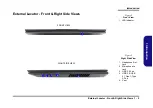
Страница 17: ...5 1 Introduction External Locator Front Right Side Views Figure 2 Front View 1 LED Indicator Figure 3 Right Side View 1 Headphone Out Jack 2 Microphone In Jack 3 USB 2 0 Port 4 USB 3 0 USB 3 1 Gen 1 Type A Port 5 Vent FRONT VIEW 1 RIGHT SIDE VIEW 1 2 3 4 5 ...

Страница 18: ...tor Left Side Rear View Figure 4 Left Side View 1 Security Lock Slot 2 DC In Jack 3 RJ 45 LAN Jack 4 Mini Display Port 5 HDMI Out Port 6 USB 3 1 Gen 2 Type C Port 7 USB 3 1 Gen 2 Type A Port 8 Multi in 1 Card Reader LEFT SIDE VIEW 1 2 3 4 5 6 7 8 Figure 5 Rear View 1 Vent REAR VIEW 1 ...

Страница 19: ...tom View 1 7 1 Introduction External Locator Bottom View Figure 6 Bottom View 1 Battery 2 Vent 3 Speakers Overheating To prevent your com puter from overhea ting make sure no thing blocks any vent while the computer is in use 2 1 3 2 3 ...

Страница 20: ...Introduction 1 8 Mainboard Overview Top Key Parts 1 Introduction Mainboard Overview Top Key Parts Figure 7 Mainboard Top Key Parts 1 KBC ITE IT8587 1 ...

Страница 21: ...Key Parts 1 9 1 Introduction Mainboard Overview Bottom Key Parts 1 2 3 4 5 6 7 Figure 8 Mainboard Bottom Key Parts 1 GPU 2 CPU 3 Memory Slots DDR4 SO DIMM 4 Mini Card Connector WLAN Module 5 PCH 6 CMOS Battery 7 M 2 Card Connector SSD Module ...

Страница 22: ...ard Overview Top Connectors Figure 9 Mainboard Top Connectors 1 DC In Jack 2 RJ 45 LAN Jack 3 External Display Port 4 HDMI Out Port 5 USB Port 3 0 3 1 Type C Connector 6 USB Port 3 0 3 1 Type A Connector 7 Multi in 1 Card Reader 8 Keyboard Cable Connector 10 7 8 6 5 1 2 3 4 ...

Страница 23: ...rd Overview Bottom Connectors 1 11 1 Introduction Mainboard Overview Bottom Connectors Figure 10 Mainboard Bottom Connectors 1 CCD Connector 2 Fan Connector 3 HDD Connector 4 Speaker Connector 5 LCD Connector 1 2 5 3 2 4 4 ...

Страница 24: ...Introduction 1 12 1 Introduction ...

Страница 25: ...sassembly process easier each section may have a box in the page margin Information contained under the figure will give a synopsis of the sequence of procedures involved in the disassembly procedure A box with a lists the relevant parts you will have after the disassembly process is complete Note The parts listed will be for the dis assembly procedure listed ONLY and not any previous disassembly ...

Страница 26: ...c ing the connection make sure the connector is oriented in the same way The pin1 side is usually not indicated Pressure sockets for multi wire connectors To release this connector type grasp it at its head and gently rock it from side to side as you pull it out Do not pull on the wires themselves When replacing the connection do not try to force it The socket only fits one way Pressure sockets fo...

Страница 27: ...the computer When handling a printed circuit board do not use gloves or other materials which allow static electricity buildup We suggest that you use an anti static wrist strap instead 8 Beware of corrosion As you perform your job avoid touching any connector leads Even the cleanest hands produce oils which can attract corrosive elements 9 Keep your work environment clean Tobacco smoke dust or ot...

Страница 28: ...e the HDD page 2 7 To remove the System Memory 1 Remove the battery page 2 5 2 Remove the HDD page 2 7 3 Remove the system memory page 2 9 To remove the M 2 SSD 1 Remove the battery page 2 5 2 Remove the HDD page 2 7 3 Remove the SSD page 2 10 To remove the Wireless LAN Module 1 Remove the battery page 2 5 2 Remove the HDD page 2 7 3 Remove the WLAN page 2 11 To remove the Heatsink 1 Remove the ba...

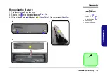
Страница 29: ...the arrow Figure 1a 3 Slide the latch in the direction of the arrow 4 While holding the latch lift the battery Figure 1b out of the compartment Figure 1c 1 2 2 3 Figure 1 Battery Removal a Slide the latch in the direction of the arrow and slide the latch in the direction of the arrow b Lift the battery c Remove the battery 1 2 1 a b 3 c 3 2 3 Battery ...

Страница 30: ...ng collar socket by using a flat head screwdriver to pry the locking collar pins away from the base Figure 2b 5 Carefully lift the keyboard off the computer Figure 2c 1 2 3 4 5 6 7 7 8 6 a b 1 2 c 6 3 4 5 6 7 8 8 7 8 8 4 Eject Stick 6 Keyboard 2 Screws Figure 2 Keyboard Removal a Remove the screws from the bottom of the compu ter and then eject the keyboard using a special eject stick to push the ...

Страница 31: ...attery page 2 5 2 Remove the SD card cover and screws Figure 3a 3 Carefully push to release the bottom case from point and then lift it up from point to release the bottom case and ports as indicated by the arrows Figure 3b 4 The HDD will be visible at point on the mainboard Figure 3c 6 1 2 17 18 19 20 21 2 a b 1 3 4 5 18 13 21 6 7 8 9 11 12 14 15 10 c 18 19 16 20 17 Figure 3 HDD Assembly Removal ...

Страница 32: ...ing New HDD s are blank Before you begin make sure You have backed up any data you want to keep from your old HDD You have all the CD ROMs and FDDs required to install your operating system and programs If you have access to the internet download the latest application and hardware driver updates for the operating system you plan to install Copy these to a removable medium g 27 22 23 24 25 24 f 24...

Страница 33: ...elease the second module if necessary 5 Insert a new module holding it at about a 30 angle and fit the connectors firmly into the memory slot 6 The module will only fit one way as defined by its pin alignment Make sure the module is seated as far into the slot as it will go DO NOT FORCE IT it should fit without much pressure 7 Press the module in and down towards the mainboard until the slot lever...

Страница 34: ...emove the battery page 2 5 and the bottom cover page 2 7 2 The M 2 SSD module will be visible at point on the mainboard Figure 6a 3 Remove the screw Figure 6b 4 The M 2 SSD module Figure 6c will pop up and you can remove it from the computer 1 2 3 b c a 2 3 1 3 3 M2 SSD Module 1 Screw Figure 6 M 2 SSD Module Removal a Locate the M 2 SSD b Remove the screw c The M 2 SSD module will pop up ...

Страница 35: ...n the mainboard Figure 7a 3 Carefully disconnect the cables and then remove the screw Figure 7b 4 The Wireless LAN module Figure 7c will pop up and you can remove it from the computer 1 2 3 4 5 b c a 2 3 5 1 5 4 5 Wireless LAN Module 1 Screw Figure 7 Wireless LAN Module Removal a Locate the WLAN b Disconnect the cables and remove the screw c The WLAN module will pop up Note Make sure you reconnect...

Страница 36: ...odules are not labelled The cables covers each cable will have either a black or transparent cable cover are color coded for identification as outlined in the table below Cable 1 is usually connected to antenna 1 Main on the module and cable 2 to antenna 2 Aux Module Type Antenna Type Cable Color Cable Cover Type WLAN WLAN Bluetooth Combo WM 1 Black Transparent WM 2 Black White ...

Страница 37: ... 2 5 and the bottom cover page 2 7 2 Loosen the CPU heat sink screws in the order the reverse order as indicated Figure 8a 3 Apply pressure to points to lift carefully it may be hot the heat sink off the mainboard Figure 8b 7 6 5 4 3 2 1 A C D Figure 8 Heat Sink Removal a Remove the screws b Carefully remove the heat sink unit 1 3 2 5 7 6 4 A B D a b C D Heat Sink 7 Screws ...

Страница 38: ...lift at the upper point as indicated by the arrows and slightly push and lift up the inner frame at the middle points as indicated by the arrows and then run your fingers around the inner frame at the lower point as indicated by the arrows Figure 9a 4 Remove the LCD front cover Figure 9b 1 2 3 4 5 6 7 8 5 b a 9 6 2 1 8 7 5 4 3 9 LCD Front Cover 2 Screws Figure 9 CCD Removal a Remove rubber and scr...

Страница 39: ...Disassembly 5 Disconnect the cable Figure 10c 6 Remove the CCD module Figure 10d 7 Reverse the process to install a new CCD module 10 11 d c 11 10 11 CCD Module Figure 10 CCD Removal cont d c Disconnect the cable d Remove the CCD mod ule ...

Страница 40: ...Disassembly 2 16 2 Disassembly ...

Страница 41: ...bers Your organization may use a different system so be sure to cross check any relevant documentation Note Some assemblies may have parts in common especially screws However the part lists DO NOT indicate the total number of duplicated parts used Note Be sure to check any update notices The parts shown in these illustrations are appropriate for the system at the time of publication Over the produ...

Страница 42: ... Illustration Location The following table indicates where to find the appropriate part list illustration Table A 1 Part List Illustration Location Part Top page A 3 Bottom page A 4 Main Board page A 5 HDD page A 6 LCD page A 7 ...

Страница 43: ...Top A 3 A Part Lists Top Figure A 1 Top ...

Страница 44: ...A 4 Bottom A Part Lists Bottom Figure A 2 Bottom ...

Страница 45: ...Main Board A 5 A Part Lists Main Board Figure A 3 Main Board ...

Страница 46: ...A 6 HDD A Part Lists HDD Figure A 4 HDD ...

Страница 47: ...LCD A 7 A Part Lists LCD Figure A 5 LCD ...

Страница 48: ...A 8 A Part Lists ...

Страница 49: ...d Page B 34 Hall Sensor Board Page B 57 VGA Frame Buffer Interface Page B 12 M 2 WLAN BT SSD Page B 35 Click Board Page B 58 VGA Frame Buffer A Page B 13 USB Conn USB Charger Page B 36 LED Board Page B 59 VGA Frame Buffer A Page B 14 Card Reader LAN RTL8411B Page B 37 Finger Print Board Page B 60 VGA Frame Buffer B Page B 15 HDD Click TP Audio Hall Con Page B 38 Power Sequence Page B 61 VGA Frame ...

Страница 50: ...B3 0 USB3 1 USB3 PORT1 USB3 PORT3 4 SHEET 35 USB3 0 USB3 1 USB2 0 PORT8 USB2 0 PORT3 USB2 0 PORT1 SATA PORT4 2400 2666 MHz DDR4 1 2V Optional SHEET 38 TPM 2 0 AC IN SHEET 49 VCCSA SHEET 53 PEX_VDD 1 8VA 1V8_AON 1V8_RUN SHEET 50 AC_IN Charger SMB BUS Nvidia N17P G0 G1 RAM SIZE 2GB 512x16x2 DDR5 908 Balls SHEET 10 11 12 13 14 15 16 17 18 19 nVIDIA Mini DP SHEET 20 HDMI SHEET 23 NGFF M Key PCIE 4X SS...

Страница 51: ...arch 02 2018 ᙔ Ϻ ႝ တ DMFWP DP SCHEMATIC1 R317 20_1 _04 C589 0 22u_10V_X5R_04 C579 0 22u_10V_X5R_04 C575 0 22u_10V_X5R_04 C577 0 22u_10V_X5R_04 C574 0 22u_10V_X5R_04 C547 0 22u_10V_X5R_04 3 OF 13 U30C CFL_H_62_INT_IP_CRB_CFLH PEG_RXP_0 E25 PEG_RXN_0 D25 PEG_RXP_1 E24 PEG_RXN_1 F24 PEG_RXP_2 E23 PEG_RXN_2 D23 PEG_RXP_3 E22 PEG_RXN_3 F22 PEG_RXP_4 E21 PEG_RXN_4 D21 PEG_RXP_5 E20 PEG_RXN_5 F20 PEG_RXP...

Страница 52: ... AR10 DDR1_CAA_2 DDR1_MA_6 AN7 DDR1_CKP_0 DDR1_CKP_0 AM9 NC DDR1_MA_4 AL6 DDR1_CAB_2 DDR1_MA_14 AH11 DDR1_DQ_15 DDR0_DQ_31 BJ7 DDR1_DQ_13 DDR0_DQ_29 BJ10 DDR1_DQ_17 DDR0_DQ_49 BG10 DDR1_CAB_8 DDR1_MA_1 AK6 DDR1_DQSN_4 DDR1_DQSN_2 AC9 DDR1_DQ_34 DDR1_DQ_18 AC11 DDR1_DQ_36 DDR1_DQ_20 AA7 DDR1_DQSP_6 DDR1_DQSP_6 P9 DDR1_DQ_60 DDR1_DQ_60 L10 DDR1_DQ_19 DDR0_DQ_51 BF8 DDR1_CKN_1 DDR1_CKN_1 AM8 DDR1_CAB...

Страница 53: ...53 VCCIO 2 6 43 1 05_VCCST 6 26 47 48 H_PROCHOT 47 PCH_CPU_BCLK_R_DN 29 PCH_CPU_BCLK_R_DP 29 PCH_CPU_PCIBCLK_R_DN 29 PCH_CPU_PCIBCLK_R_DP 29 CPU_24MHZ_R_DN 29 CPU_24MHZ_R_DP 29 H_PWRGD 27 PLTRST_CPU_N 26 H_PM_SYNC 26 H_SKTOCC_N 28 DDR_VTT_PG_CTRL 45 H_CPU_SVIDCLK 47 H_CPU_SVIDDAT 47 H_CPU_SVIDALRT 47 PCH_THERMTRIP 26 PCH_PECI 26 H_PM_DOWN 26 H_PECI 40 3 3VA 9 24 26 27 30 48 ALL_SYS_PWRGD 22 25 40 ...

Страница 54: ...C91 AL32 VCC80 AK32 VCC3 AA32 VCC90 AL31 VCC_SENSE AG37 VCC19 AC14 VCC2 AA31 VCC29 AD14 VCC18 AC13 VCC1 AA13 VCC109 AN32 VCC39 AE14 VCC28 AD13 VCC17 AB38 VCC119 AP32 VCC108 AN31 VCC49 AF31 VCC38 AE13 VCC27 AC36 VCC16 AB37 VCC118 AP31 VCC107 AN14 VCC59 AG32 VCC48 AF30 VCC37 AD38 VCC26 AC35 VCC15 AB36 VCC117 AP30 VCC106 AN13 VCC69 AH32 VCC58 AG31 VCC47 AF29 VCC36 AD37 VCC25 AC34 VCC14 AB35 VCC116 AP...

Страница 55: ...6S_08 C289 22u_6 3V_X6S_08 R76 100_04 C422 22u_6 3V_X6S_08 12 OF 13 U30L CFL_H_62_INT_IP_CRB_CFLH VCCSA1 J30 VCCSA2 K29 VCCSA3 K30 VCCSA4 K31 VCCSA5 K32 VCCSA6 K33 VCCSA7 K34 VCCSA8 K35 VCCSA9 L31 VCCSA10 L32 VCCSA11 L35 VCCSA12 L36 VCCSA13 L37 VCCSA14 L38 VCCSA15 M29 VCCSA16 M30 VCCSA17 M31 VCCSA18 M32 VCCSA19 M33 VCCSA20 M34 VCCSA21 M35 VCCSA22 M36 VCCIO1 AG12 VCCIO2 G15 VCCIO3 G17 VCCIO4 G19 VC...

Страница 56: ...8 VSS_281 BM2 VSS_282 BM21 VSS_283 BM22 VSS_284 BM23 VSS_285 BM24 VSS_286 BM25 VSS_287 BM26 VSS_288 BM27 VSS_289 BM28 VSS_290 BM29 VSS_291 BM3 VSS_292 BM33 VSS_293 BM35 VSS_294 BM38 VSS_295 BM5 VSS_296 BM6 VSS_297 BM7 VSS_298 BM8 VSS_299 BM9 VSS_300 BN12 VSS_301 BN14 VSS_302 BN18 VSS_303 BN19 VSS_304 BN2 VSS_305 BN20 VSS_306 BN21 VSS_307 BN24 VSS_308 BN29 VSS_309 BN30 VSS_310 BN31 VSS_311 BN34 VSS...

Страница 57: ... 10u_6 3V_X5R_06 R173 1K_1 _04 C385 10u_6 3V_X5R_06 R182 24 9_1 _04 C840 1u_6 3V_X5R_04 C373 0 1u_10V_X7R_04 R172 1K_1 _04 C668 1u_6 3V_X5R_04 C675 1u_6 3V_X5R_04 C376 0 1u_10V_X5R_04 C371 10u_6 3V_X5R_06 C398 10u_6 3V_X5R_06 C669 1u_6 3V_X5R_04 C670 1u_6 3V_X5R_04 C377 2 2u_6 3V_X5R_04 R181 240_1 _04 J_DIMMA_1B D4AR0 26001 1P52 VDD19 163 VDD18 160 VDD17 159 VDD16 154 VDD15 153 VDD14 148 VDD13 147...

Страница 58: ... C699 0 1u_10V_X7R_04 R475 1K_1 _04 C380 1u_6 3V_X5R_04 C697 0 1u_10V_X7R_04 R473 2_1 _04 R207 240_1 _04 J_DIMMB_2B D4AS0 26001 1P52 VDD19 163 VDD18 160 VDD17 159 VDD16 154 VDD15 153 VDD14 148 VDD13 147 VDD12 142 VDD11 141 VDD10 136 VDD9 135 VDD8 130 VDD7 129 VDD6 124 VDD5 123 VDD4 118 VDD3 117 VDD2 112 VDD1 111 VSS 251 VSS 247 VSS 243 VSS 239 VSS 235 VSS 231 VSS 227 VSS 223 VSS 217 VSS 213 VSS 20...

Страница 59: ...C AJ28 NC AC6 NC M8 3V3_MAIN L8 3V3_MAIN K8 3V3_AON J8 3V3_AON C30 4 7u_6 3V_X6S_06 C65 0 1u_10V_X7R_04 NV FOOTPRINT R329 100K_04 C198 0 1u_10V_X7R_04 C47 0 22u_10V_X5R_04 R65 100K_04 1 19 PCI_EXPRESS N17P GB4C 128 PEX_DVDD PEX_DVDD PEX_DVDD PEX_DVDD PEX_DVDD PEX_DVDD PEX_HVDD PEX_HVDD PEX_HVDD PEX_HVDD PEX_HVDD PEX_HVDD PEX_HVDD PEX_HVDD PEX_HVDD PEX_HVDD PEX_HVDD PEX_HVDD PEX_HVDD PEX_HVDD N17P ...

Страница 60: ...30 FBB_DQM6 F27 FBB_DQM5 F23 FBB_DQM4 C9 FBB_DQM3 A3 FBB_DQM2 E3 FBB_DQM1 E11 FBB_DQM0 C26 FBB_D63 B26 FBB_D62 C24 FBB_D61 B24 FBB_D60 C21 FBB_D59 A21 FBB_D58 C23 FBB_D57 B21 FBB_D56 B29 FBB_D55 C29 FBB_D54 A29 FBB_D53 D29 FBB_D52 B32 FBB_D51 C32 FBB_D50 C31 FBB_D49 A32 FBB_D48 D30 FBB_D47 E30 FBB_D46 F29 FBB_D45 E29 FBB_D44 E27 FBB_D43 G26 FBB_D42 D27 FBB_D41 G27 FBB_D40 F21 FBB_D39 G21 FBB_D38 E...

Страница 61: ... B11 DQ10 A13 DQ9 A11 DQ8 D2 DBI0 C2 EDC0 F2 DQ7 F4 DQ6 E2 DQ5 E4 DQ4 B2 DQ3 B4 DQ2 A2 DQ1 A4 DQ0 A10 VREFD R338 549_1 _04 COMMON BGA170 INS1220714 U151B K4G41325FE HC28 J10 SEN J13 ZQ J14 VREFC V5 NC_RFU_V5 A5 NC_RFU_A5 J11 CLK J12 CLK J3 CKE J2 RESET J5 RFU_A12 K4 A7_A8 K5 A6_A11 K10 A5_BA1 K11 A4_BA2 H10 A3_BA3 H11 A2_BA0 H5 A1_A9 H4 A0_A10 J4 ABI G12 CS L12 WE L3 CAS G3 RAS add 1k to VSS Norma...

Страница 62: ...12 WE G3 CAS L3 RAS C33 0 1u_10V_X7R_04 R285 931_1 _04 C121 1u_6 3V_X6S_04 C123 1u_6 3V_X6S_04 R284 1K_04 NC NC NC NC NC NC NC NC GND x32 x16 MIRRORED NC COMMON BGA170_MIRR INS1226066 U152A K4G41325FE HC28 CHANGE D5 WCK23 D4 WCK23 D2 DBI3 C2 EDC3 F2 DQ31 F4 DQ30 E2 DQ29 E4 DQ28 B2 DQ27 B4 DQ26 A2 DQ25 A4 DQ24 D13 DBI2 C13 EDC2 F13 DQ23 F11 DQ22 E13 DQ21 E11 DQ20 B13 DQ19 B11 DQ18 A13 DQ17 A11 DQ16...

Страница 63: ...0 C2 EDC0 F2 DQ7 F4 DQ6 E2 DQ5 E4 DQ4 B2 DQ3 B4 DQ2 A2 DQ1 A4 DQ0 A10 VREFD COMMON BGA170 INS1233936 U158B K4G41325FE HC28 N16P GT J10 SEN J13 ZQ J14 VREFC V5 NC_RFU_V5 A5 NC_RFU_A5 J11 CLK J12 CLK J3 CKE J2 RESET J5 RFU_A12 K4 A7_A8 K5 A6_A11 K10 A5_BA1 K11 A4_BA2 H10 A3_BA3 H11 A2_BA0 H5 A1_A9 H4 A0_A10 J4 ABI G12 CS L12 WE L3 CAS G3 RAS C635 0 1u_10V_X7R_04 R375 1 33K_1 _04 C633 0 1u_10V_X7R_04...

Страница 64: ...H2 VSSQ H13 VSSQ F5 VSSQ F10 VSSQ E3 VSSQ E14 VSSQ E12 VSSQ E1 VSSQ C4 VSSQ C3 VSSQ C14 VSSQ C12 VSSQ C11 VSSQ C1 VSSQ A3 VSSQ A14 VSSQ A12 VSSQ A1 VSSQ T5 VSS T10 VSS P10 VSS L5 VSS L10 VSS K14 VSS K1 VSS H14 VSS H1 VSS G5 VSS G10 VSS D10 VSS B5 VSS B10 VSS T3 VDDQ T14 VDDQ T12 VDDQ T1 VDDQ P3 VDDQ P14 VDDQ P12 VDDQ P1 VDDQ N5 VDDQ N10 VDDQ M3 VDDQ M14 VDDQ M12 VDDQ M1 VDDQ L2 VDDQ L13 VDDQ K3 VD...

Страница 65: ...SDA T4 I2CS_SCL DP DVI SL HDMI DVI DL TXD2 TXD2 TXD2 TXD1 TXD0 TXD0 TXD1 I2CZ_SCL I2CZ_SDA TXC TXC HPD_F HPD_E TXC TXC TXD0 TXD0 TXD1 TXD1 TXD2 I2CY_SDA I2CY_SCL I2CY_SCL I2CY_SDA TXD2 TXD2 TXD0 TXD0 TXC TXC TXD1 TXD1 HPD_E TXD3 TXD3 TXD4 TXD4 TXD5 TXD5 IFPE IFPF 9 19 IFPEF ALL PINS NC FOR GF117 IFPE_AUX_SCL IFPE_AUX_SDA_N N17P GB4C 128 N17P GB4C 128 IFP_IOVDD IFP_IOVDD IFPF_AUX_SCL IFPF_AUX_SDA_N...

Страница 66: ..._EN 16 NV_OVERT 16 1V8_AON_PWRGD 53 PLT_RST 24 25 DGPU_RST _PCH 28 NV_NVVDD_EN 51 NVVDD_PWRGD 10 51 Title Size Document Number R e v Date Sheet of 6 71 N85J0 D01 D02B 17 NVIDIA POWER SEQUENCE Custom 17 63 Friday March 02 2018 ᙔ Ϻ ႝ တ DMFWP DP SCHEMATIC1 Title Size Document Number R e v Date Sheet of 6 71 N85J0 D01 D02B 17 NVIDIA POWER SEQUENCE Custom 17 63 Friday March 02 2018 ᙔ Ϻ ႝ တ DMFWP DP SCH...

Страница 67: ...1V8_MAIN GPPG9_PCH_NV3V3_EN GPP_G9 NV3V3 GPPG10_PCH_NVVDD_EN GPP_G10 NVVDD GPPG11_PCH_NVVDDS_EN GPP_G11 NVVDDS GPPG0_PCH_PEXVDD_EN GPP_G0 PEX_VDD net PCH_GPIO Voltage DGPU_PWR_EN GPP_F23 1V8_AON POWER RAIL State in GC6 1V8_AON 1V8_MAIN PEX 1 05V NVVDD ON OFF OFF OFF FBVDD Q ON NVVDDS OFF 9 13 Common Design D02_12 19_H 1V8_AON 1V8_AON 10 16 17 51 52 53 GPIO4_1V8_MAIN_EN 16 17 GPIO4_1V8_MAIN_EN_R 24...

Страница 68: ...5 1u_6 3V_X6S_04 NV FOOTPRINT C531 22u_6 3V_X6S_08 C144 4 7u_6 3V_X6S_06 NV FOOTPRINT C103 1u_6 3V_X6S_04 NV FOOTPRINT C150 1u_6 3V_X6S_04 NV FOOTPRINT C140 4 7u_6 3V_X6S_06 NV FOOTPRINT C532 22u_6 3V_X6S_08 C84 4 7u_6 3V_X6S_06 C152 4 7u_6 3V_X6S_06 NV FOOTPRINT C500 4 7u_6 3V_X6S_06 C102 4 7u_6 3V_X6S_06 NV FOOTPRINT C142 4 7u_6 3V_X6S_06 NV FOOTPRINT C146 1u_6 3V_X6S_04 NV FOOTPRINT C91 4 7u_6 ...

Страница 69: ...2018 ᙔ Ϻ ႝ တ DMFWP DP SCHEMATIC1 Title Size Document Number Re v Date Sheet o f 6 71 N85J0 D01 D02B 20 MDP iGPU A3 20 63 Friday March 02 2018 ᙔ Ϻ ႝ တ DMFWP DP SCHEMATIC1 C75 0 1u_10V_X7R_04 S D G Q26A MTDK3S6R 2 6 1 S D G Q31B MTDK3S6R 5 3 4 S D G Q29A MTDK3S6R 2 6 1 S D G Q26B MTDK3S6R 5 3 4 S D G Q29B MTDK3S6R 5 3 4 R303 100K_1 _04 S D G Q27A MTDK3S6R 2 6 1 C74 0 1u_10V_X7R_04 C36 10u_6 3V_X5R_0...

Страница 70: ...y March 02 2018 Title Size Document Number Re v Date Sheet o f 6 71 N85J0 D01 D02B 21 MDP dGPU A3 21 63 Friday March 02 2018 Title Size Document Number Re v Date Sheet o f 6 71 N85J0 D01 D02B 21 MDP dGPU A3 21 63 Friday March 02 2018 D5 DT1140 04LP 7 5 1 2 3 4 10 9 8 7 6 D7 DT1140 04LP 7 5 1 2 3 4 10 9 8 7 6 C221 0 1u_10V_X7R_04 C129 0 1u_10V_X7R_04 C169 0 1u_10V_X7R_04 S D G Q22B MTDK3S6R 5 3 4 S...

Страница 71: ...TIC1 Title Size Document Number Re v Date Sheet o f 6 71 N85J0 D01 D02B 22 PANEL INVERTER A3 22 63 Friday March 02 2018 ᙔ Ϻ ႝ တ DMFWP DP SCHEMATIC1 C556 0 1u_10V_X7R_04 R353 0_04 C564 0 1u_10V_X7R_04 R69 100K_04 R71 100K_04 C614 0 01u_50V_X7R_04 C557 0 1u_10V_X7R_04 U36B 74LVC08APW 4 5 6 14 7 C565 0 1u_10V_X7R_04 Q8B MTS3572G6 S1 2 D1 6 G1 1 C558 0 1u_10V_X7R_04 C250 0 22u_50V_Y5V_06 R354 100K_04 ...

Страница 72: ...DATA2J TMDS_DATA2 TMDS_DATA2 HDMI_HPD C HDMI_HPD HDMI_CTRLDATA HDMI_CTRLCLK HDMI_SCL C HDMI_SDA C HDMI_SCL C HDMI_SDA C HDMI_HPD C 5VS HDMI_5VS GND 5VS 5VS 3 3VS HDMI_5VS HDMI_5VS HDMI_DATA0P 2 HDMI_DATA0N 2 HDMI_DATA2P 2 HDMI_DATA2N 2 HDMI_CLOCKP 2 HDMI_DATA1P 2 HDMI_CLOCKN 2 HDMI_DATA1N 2 SUSB 20 21 37 42 5VS 9 20 21 37 38 39 40 41 42 51 3 3VS 8 9 20 21 22 24 26 27 28 29 32 34 36 37 38 39 40 41 ...

Страница 73: ... D02B 24 PCH 1 12 SPI SMBUS A3 24 63 Friday March 02 2018 ᙔ Ϻ ႝ တ DMFWP DP SCHEMATIC1 Title Size Document Number Re v Date Sheet o f 6 71 N85J0 D01 D02B 24 PCH 1 12 SPI SMBUS A3 24 63 Friday March 02 2018 ᙔ Ϻ ႝ တ DMFWP DP SCHEMATIC1 R138 0_04 PJ48 1mm 1 2 R434 33_04 R154 10K_04 R430 4 7K_04 R128 100K_04 R436 33_04 R165 10K_04 R404 4 7K_04 R129 4 7K_04 R159 33_04 R699 20K_04 T35 C678 0 1u_10V_X7R_0...

Страница 74: ...B2 0 A3 25 63 Friday March 02 2018 ᙔ Ϻ ႝ တ DMFWP DP SCHEMATIC1 2 OF 13 U34B HM370 USB2N_1 J3 USB2P_1 J2 USB2N_2 N13 USB2P_2 N15 USB2N_3 K4 USB2P_3 K3 USB2N_4 M10 USB2P_4 L9 USB2N_5 M1 USB2P_5 L2 USB2N_6 K7 USB2P_6 K6 USB2N_7 L4 USB2P_7 L3 USB2N_8 G4 USB2P_8 G5 USB2N_9 M6 USB2P_9 N8 USB2N_10 H3 USB2P_10 H2 USB2N_11 R10 USB2P_11 P9 USB2N_12 G1 USB2P_12 G2 USB2N_13 N3 USB2P_13 N2 USB2N_14 E5 USB2P_14...

Страница 75: ...P DP SCHEMATIC1 R389 10K_04 R397 1K_04 R407 10K_04 R399 12 1_1 _04 C600 0 22u_10V_X5R_04 T97 R400 30 1_1 _04 T106 R398 30 1_1 _04 R416 10K_04 C605 0 1u_10V_X7R_04 T104 C601 0 22u_10V_X5R_04 C596 0 22u_10V_X5R_04 C603 0 1u_10V_X7R_04 C606 0 1u_10V_X7R_04 T110 C602 0 22u_10V_X5R_04 T107 C604 0 1u_10V_X7R_04 R132 100K_04 T115 T17 C595 0 22u_10V_X5R_04 T116 R417 10K_04 T114 T96 R420 10K_04 T95 T149 3 ...

Страница 76: ...March 02 2018 ᙔ Ϻ ႝ တ DMFWP DP SCHEMATIC1 Title Size Document Number Re v Date Sheet o f 6 71 N85J0 D01 D02B 27 PCH 4 12 HDA SMBUS RTC A3 27 63 Friday March 02 2018 ᙔ Ϻ ႝ တ DMFWP DP SCHEMATIC1 Title Size Document Number Re v Date Sheet o f 6 71 N85J0 D01 D02B 27 PCH 4 12 HDA SMBUS RTC A3 27 63 Friday March 02 2018 ᙔ Ϻ ႝ တ DMFWP DP SCHEMATIC1 R413 30 1_1 _04 R146 0_04 Q20 2SK3018S3 G D S C360 1u_6 ...

Страница 77: ... DPP ESPI USB3 0 A3 28 63 Friday March 02 2018 ᙔ Ϻ ႝ တ DMFWP DP SCHEMATIC1 Title Size Document Number Re v Date Sheet o f 6 71 N85J0 D01 D02B 28 PCH 5_6 12 DPP ESPI USB3 0 A3 28 63 Friday March 02 2018 ᙔ Ϻ ႝ တ DMFWP DP SCHEMATIC1 5 OF 13 U34E HM370 GPP_K22 IMGCLKOUT0 L48 GPP_F14 EXT_PWR_GATE PS_ON AP41 GPP_F22 DDPF_CTRLCLK AT49 GPP_I1 DDPC_HPD1 DISP_MISC1 AN10 GPP_I10 DDPD_CTRLDATA AR3 GPP_K23 IMG...

Страница 78: ...nt Number Re v Date Sheet o f 6 71 N85J0 D01 D02B 29 PCH 7 12 CLKOUT A3 29 63 Friday March 02 2018 ᙔ Ϻ ႝ တ DMFWP DP SCHEMATIC1 L31 FCM1005KF 121T03 1 2 C835 5p_50V_NPO_04 C661 15p_50V_NPO_04 C657 15p_50V_NPO_04 R386 1M_1 _04 C649 15p_50V_NPO_04 RN1 10K_8P4R_04 1 2 3 4 5 6 7 8 R452 10M_06 7 OF 13 U34G HM370 CLKOUT_CPUNSSC_P D7 CLKOUT_CPUBCLK_P B8 XTAL_OUT U9 XTAL_IN U10 XCLK_BIASREF T3 RTCX1 BA49 R...

Страница 79: ...heet o f 6 71 N85J0 D01 D02B 30 PCH 8 12 POWER A3 30 63 Friday March 02 2018 ᙔ Ϻ ႝ တ DMFWP DP SCHEMATIC1 Title Size Document Number Re v Date Sheet o f 6 71 N85J0 D01 D02B 30 PCH 8 12 POWER A3 30 63 Friday March 02 2018 ᙔ Ϻ ႝ တ DMFWP DP SCHEMATIC1 R95 0402_short p C625 1u_6 3V_X5R_04 R98 0402_short p C315 22u_6 3V_X5R_06 PJ9 4mm 1 2 C312 22u_6 3V_X5R_06 R450 0402_short p C358 1u_6 3V_X5R_04 R97 04...

Страница 80: ...VSS_68 AK28 VSS_57 AJ19 VSS_46 AG22 VSS_35 AD25 VSS_24 AB31 VSS_13 AA19 VSS_6 A4 VSS_142 BG22 VSS_131 BC45 VSS_120 BB43 VSS_69 AK30 VSS_58 AJ20 VSS_47 AG23 VSS_36 AD49 VSS_25 AC12 VSS_14 AA20 VSS_7 A45 VSS_143 BG25 VSS_132 BC8 VSS_121 BB9 VSS_110 AW46 VSS_59 AJ25 VSS_48 AG25 VSS_37 AE12 VSS_26 AC17 VSS_15 AA25 VSS_8 A46 VSS_144 BG28 VSS_133 BD43 VSS_122 BC10 VSS_111 B47 VSS_100 AT26 VSS_49 AG27 VS...

Страница 81: ...M370 TRIGGER_OUT AK3 TRIGGER_IN AK2 CPU_TRST AM4 PREQ AL2 RSVD8 Y15 RSVD7 Y14 RSVD6 U37 RSVD5 U35 RSVD4 R32 RSVD3 N32 PRDY AM5 RSVD2 AH15 RSVD1 AH14 T45 11 OF 13 U34K HM370 GPP_B21 GSPI1_MISO BD30 GPP_C22 UART2_RTS AW21 GPP_C8 UART0_RXD BE23 GPP_C20 UART2_RXD BD20 GPP_D13 ISH_UART0_RXD I2C2_SDA BE17 GPP_C10 UART0_RTS BA24 GPP_C23 UART2_CTS AV21 GPP_B22 GSPI1_MOSI BA26 GPP_D12 ISH_SPI_MOSI GP_BSSB_...

Страница 82: ... 3 4 4 C4 0 1u_10V_X7R_04 C814 0 1u_10V_X7R_04 LTE H28 H6_5D3_7 LTE C813 0 1u_10V_X7R_04 LTE R424 10_06 LTE R691 0_06 LTE C815 470p_50V_X7R_04 LTE T146 Q34A MTS3572G6 LTE S2 4 D2 3 G2 5 Q35 2SK3018S3 LTE G D S C562 0 1u_10V_X7R_04 LTE Q34B MTS3572G6 LTE S1 2 D1 6 G1 1 C5 22p_50V_NPO_04 R419 100K_04 LTE R8 4 7K_04 LTE C816 0 1u_10V_X7R_04 LTE B KEY J_3G1 NFSB0 S6701 TP40 PCB Footprint NXSB0 S67XX X...

Страница 83: ...N85J0 D01 D02B 34 M 2 WLAN BT PCIE4X SSD A3 34 63 Friday March 02 2018 ᙔ Ϻ ႝ တ DMFWP DP SCHEMATIC1 Title Size Document Number Re v Date Sheet o f 6 71 N85J0 D01 D02B 34 M 2 WLAN BT PCIE4X SSD A3 34 63 Friday March 02 2018 ᙔ Ϻ ႝ တ DMFWP DP SCHEMATIC1 C389 0 1u_10V_X5R_04 R440 75K_1 _04 R168 10K_04 U13 UP7553PMA5 25 EN 3 VIN 5 VIN SS 4 VOUT 1 GND 2 E KEY J_WLAN1 NFSE0 S6701 TP40 SUSCLK 32Khz O 50 CL...

Страница 84: ...WP DP SCHEMATIC1 Title Size Document Number Re v Date Sheet o f 6 71 N85J0 D01 D02B 35 USB3 0 CON USB CHARGER Custom 35 63 Friday March 02 2018 ᙔ Ϻ ႝ တ DMFWP DP SCHEMATIC1 Title Size Document Number Re v Date Sheet o f 6 71 N85J0 D01 D02B 35 USB3 0 CON USB CHARGER Custom 35 63 Friday March 02 2018 ᙔ Ϻ ႝ တ DMFWP DP SCHEMATIC1 D42 TEA10402V15A0 1 2 Q43 2SK3018S3 G D S ER3 0_04 R696 4 7K_04 R176 0_04...

Страница 85: ... 40 LAN_WAKEUP 27 40 3 3VS 8 9 20 21 22 23 24 26 27 28 29 32 34 37 38 39 40 41 42 47 51 52 53 3 3V 2 17 22 33 35 42 43 45 47 48 VDD3 4 24 25 27 30 34 37 40 42 43 44 48 50 51 52 53 Title Size Document Number Re v Date Sheet o f 6 71 N85J0 D01 D02B 36 CARD READER LAN RTL8411B A3 36 63 Friday March 02 2018 ᙔ Ϻ ႝ တ DMFWP DP Title Size Document Number Re v Date Sheet o f 6 71 N85J0 D01 D02B 36 CARD REA...

Страница 86: ...mber Re v Date Sheet o f 6 71 N85J0 D01 D02B 37 HDD CLICK TP AUDIO HALL CON A3 37 63 Friday March 02 2018 ᙔ Ϻ ႝ တ DMFWP DP SCHEMATIC1 Title Size Document Number Re v Date Sheet o f 6 71 N85J0 D01 D02B 37 HDD CLICK TP AUDIO HALL CON A3 37 63 Friday March 02 2018 ᙔ Ϻ ႝ တ DMFWP DP SCHEMATIC1 Title Size Document Number Re v Date Sheet o f 6 71 N85J0 D01 D02B 37 HDD CLICK TP AUDIO HALL CON A3 37 63 Fri...

Страница 87: ...6 37 40 42 43 44 48 50 51 52 53 5VS 9 20 21 23 37 39 40 41 42 51 5V 22 35 37 42 45 46 47 48 49 52 53 SATA_LED 26 EC_SSD_LED 40 AIRPLAN_LED 40 LED_BAT_FULL 40 LED_BAT_CHG 40 LED_PWR 40 LED_ACIN 40 M2M_SSD1_LED 34 USB_PN8 25 USB_PP8 25 Title Size Document Number Re v Date Sheet o f 6 71 N85J0 D01 D02B 38 LED CCD TPM POWER SW CON A3 38 63 Friday March 02 2018 ᙔ Ϻ ႝ တ DMFWP DP SCHEMATIC1 Title Size Do...

Страница 88: ... v Date Sheet o f 6 71 N85J0 D01 D02B 39 AUDIO CODEC ALC269 VC2 A3 39 63 Friday March 02 2018 ᙔ Ϻ ႝ တ DMFWP DP SCHEMATIC1 Title Size Document Number Re v Date Sheet o f 6 71 N85J0 D01 D02B 39 AUDIO CODEC ALC269 VC2 A3 39 63 Friday March 02 2018 ᙔ Ϻ ႝ တ DMFWP DP SCHEMATIC1 Title Size Document Number Re v Date Sheet o f 6 71 N85J0 D01 D02B 39 AUDIO CODEC ALC269 VC2 A3 39 63 Friday March 02 2018 ᙔ Ϻ ...

Страница 89: ... v Date Sheet o f 6 71 N85J0 D01 D02B 40 KBC ITE IT8587 Custom 40 63 Friday March 02 2018 ᙔ Ϻ ႝ တ DMFWP DP SCHEMATIC1 Title Size Document Number Re v Date Sheet o f 6 71 N85J0 D01 D02B 40 KBC ITE IT8587 Custom 40 63 Friday March 02 2018 ᙔ Ϻ ႝ တ DMFWP DP SCHEMATIC1 R250 100K_04 C519 10u_6 3V_X5R_06 C426 1u_6 3V_X5R_04 C453 5p_50V_NPO_04 J_FAN4 85204 04001 PCB Footprint 85205 0400M 1 2 3 4 C522 100p...

Страница 90: ...SO17 40 SMC_VGA_THERM 16 40 SMD_VGA_THERM 16 40 KBLIGHT_ADJ 40 LIGHT_KB_DET 40 Title Size Document Number Re v Date Sheet o f 6 71 N85J0 D01 D02B 41 RGB KB Only 41 63 Friday March 02 2018 ᙔ Ϻ ႝ တ DMFWP DP SCHEMATIC1 A3 Title Size Document Number Re v Date Sheet o f 6 71 N85J0 D01 D02B 41 RGB KB Only 41 63 Friday March 02 2018 ᙔ Ϻ ႝ တ DMFWP DP SCHEMATIC1 A3 Title Size Document Number Re v Date Shee...

Страница 91: ... 2018 ᙔ Ϻ ႝ တ DMFWP DP SCHEMATIC1 Title Size Document Number Re v Date Sheet o f 6 71 N85J0 D01 D02B 42 5V 5VS 3 3V 3 3VS 3 3VA A3 42 63 Friday March 02 2018 ᙔ Ϻ ႝ တ DMFWP DP SCHEMATIC1 R225 1K_1 _04 R238 1_1 _06 PQ8 2SK3018S3 G D S R264 10K_04 C458 470p_50V_X7R_04 G5016 U23 CT2 10 OUT2 8 EN2 5 VBIAS 4 IN2 6 GND 11 EN1 3 CT1 12 OUT1 13 IN1 1 IN1 2 OUT1 14 IN2 7 OUT2 9 GND 15 R230 100_04 R248 10K_0...

Страница 92: ...N85J0 D01 D02B 43 VDD1 0V VCCIO A2 43 63 Friday March 02 2018 ᙔ Ϻ ႝ တ DMFWP DP SCHEMATIC1 Title Size Document Number R e v Date Sheet o f 6 71 N85J0 D01 D02B 43 VDD1 0V VCCIO A2 43 63 Friday March 02 2018 ᙔ Ϻ ႝ တ DMFWP DP SCHEMATIC1 Title Size Document Number R e v Date Sheet o f 6 71 N85J0 D01 D02B 43 VDD1 0V VCCIO A2 43 63 Friday March 02 2018 ᙔ Ϻ ႝ တ DMFWP DP SCHEMATIC1 C365 0 1u_10V_X5R_04 PD2...

Страница 93: ...8 PR318 0_06 PR316 78 7K_1 _04 PQ39 QM3004M3 4 5 2 5 5 3 1 5 S D G Q41A MTDK3S6R 2 6 1 PR309 30K_1 _06 PD19 CSOD140BSH A C PC256 4 7u_25V_X7R_08 PR310 0_06 R493 0402_short p PC257 EEEFZ1E101P 1 2 PQ43 QM3006M3 4 5 2 5 5 3 1 5 EMC13 1000p_50V_X7R_04 PC102 0 1u_25V_X7R_06 PC105 1000p_50V_X7R_04 PR314 19 1K_1 _06 PC262 4 7u_25V_X7R_08 PC258 0 1u_10V_X7R_04 PQ40 QM3004M3 4 5 2 5 5 3 1 5 PL18 BCIHP0730...

Страница 94: ... 2018 ᙔ Ϻ ႝ တ DMFWP DP SCHEMATIC1 PU3 G9661 25ADJF11U GND 8 VCNTL 4 NC 5 VIN 3 VOUT 6 VFB 7 POK 1 EN 2 GND 9 PR132 47K_04 C413 1u_6 3V_X5R_04 PR304 0603_short p C427 0 1u_10V_X7R_04 PC248 0 1u_10V_X7R_04 PQ36 MDU1516 ULTRASO 8 G D S PC249 100p_50V_NPO_04 R211 100K_04 PJ12 CV 40mil 1 2 PC91 10u_6 3V_X5R_06 PR302 402K_1 _04 EMC21 2200p_50V_X7R_04 Q15 2SK3018S3 G D S C431 0 1u_10V_X7R_04 R471 10K_04 ...

Страница 95: ...Friday March 02 2018 ᙔ Ϻ ႝ တ DMFWP DP SCHEMATIC1 PC130 0 22u_16V_X7R_06 PC59 22u_6 3V_X6S_08 PC204 2 2u_6 3V_X5R_04 PR264 2 2_06 PC116 2 2u_6 3V_X5R_04 EMC25 0 1u_25V_X7R_06 PC111 EEEFZ1E101P 1 2 PC35 1u_25V_X7R_06 PC148 4 7u_25V_X7R_08 PL9 PCMB104T R15MS 1 2 PC199 390uF_2 5V_10m_6 3 6 PC73 PSLB30E227M EMC24 0 1u_25V_X7R_06 EMC23 0 1u_25V_X7R_06 COMMON MLP08 INS29161921 PQ23 CSD87350Q5D 1 D1 2 3 G...

Страница 96: ...2B 47 VCC_CORE VCCGT A2 47 63 Friday March 02 2018 ᙔ Ϻ ႝ တ DMFWP DP SCHEMATIC1 Title Size Document Number R e v Date Sheet o f 6 71 N85J0 D01 D02B 47 VCC_CORE VCCGT A2 47 63 Friday March 02 2018 ᙔ Ϻ ႝ တ DMFWP DP SCHEMATIC1 PR187 215K_1 _04 PC155 0 1u_16V_X7R_04 PJ28 OPEN_4mil OPEN SHORT 1 2 PC44 2200p_50V_X7R_04 PR213 39 2K_1 _04 PC135 470p_50V_X7R_04 PR163 100K_1 _04 PC43 1000p_50V_X7R_04 PR61 1 ...

Страница 97: ...umber Rev Date Sheet o f 6 71 N85J0 D01 D02B 48 1 0DX_VCCSTG VCCSFR_OC 3 3VA Custom 48 63 Friday March 02 2018 ᙔ Ϻ ႝ တ DMFWP DP SCHEMATIC1 Title Size Document Number Rev Date Sheet o f 6 71 N85J0 D01 D02B 48 1 0DX_VCCSTG VCCSFR_OC 3 3VA Custom 48 63 Friday March 02 2018 ᙔ Ϻ ႝ တ DMFWP DP SCHEMATIC1 R408 0_04 C368 10u_6 3V_X5R_06 S D G PQ44A MTDK3S6R 2 6 1 C856 10u_6 3V_X5R_06 PR93 100_04 C857 1u_6 ...

Страница 98: ...Date Sheet o f 6 71 N85J0 D01 D02B 49 VCCSA A3 49 63 Friday March 02 2018 ᙔ Ϻ ႝ တ DMFWP DP SCHEMATIC1 Title Size Document Number Re v Date Sheet o f 6 71 N85J0 D01 D02B 49 VCCSA A3 49 63 Friday March 02 2018 ᙔ Ϻ ႝ တ DMFWP DP SCHEMATIC1 Title Size Document Number Re v Date Sheet o f 6 71 N85J0 D01 D02B 49 VCCSA A3 49 63 Friday March 02 2018 ᙔ Ϻ ႝ တ DMFWP DP SCHEMATIC1 EMC9 2200p_50V_X7R_04 PR242 0_...

Страница 99: ...04 PC15 0 1u_25V_X7R_06 EMC32 0 1u_25V_X7R_06 PR8 10K_04 PR13 470K_04 PQ12 2SK3018S3 G D S C3 30p_50V_NPO_04 PC8 0 1u_25V_X7R_06 PR179 10K_1 _04 PU1 BQ24780SRUYR ACN 1 ACP 2 CMSRC 3 ACDRV 4 ACOK 5 ACDET 6 IADP 7 IDCHG 8 PMON 9 PROCHOT 10 SDA 11 SCL 12 CMPIN 13 CMPOUT 14 BATPRES 15 TB_STAT 16 BATSRC 17 BATDRV 18 SRN 19 SRP 20 ILIM 21 GND_1 22 LODRV 23 REGN 24 BTST 25 HIDRV 26 PHASE 27 VCC 28 GND_2 ...

Страница 100: ...4700p_50V_X7R_04 PR202 30K_1 _04 PC182 0 1u_10V_X7R_04 PC140 0 1u_10V_X5R_04 PR39 100K_04 EMC38 0 1u_25V_X7R_06 PR204 499_1 _04 EMC34 0 1u_25V_X7R_06 PC176 390uF_2 5V_10m_6 3 6 PQ5 2SK3018S3 G D S PR200 0_04 PC125 4 7u_25V_X7R_08 PC58 8200p_50V_X7R_04 PJ25 CV 40mil 1 2 EMC41 0 01u_25V_X7R_04 EMC37 0 1u_25V_X7R_06 PR203 0_04 PL5 CMMS104T R22MS PR205 499_1 _04 PC167 0 01u_50V_X7R_04 PC142 0 1u_25V_X...

Страница 101: ..._04 PR124 0_04 PC81 0 01u_16V_X7R_04 PQ32 QM3006M3 4 5 2 5 5 3 1 5 PQ33 QM3004M3 4 5 2 5 5 3 1 5 PJ42 CV 40mil OPEN 1 2 EMC17 220p_50V_NPO_04 PJ43 CV 40mil OPEN 1 2 PQ35 2SK3018S3 G D S PR113 0_04 PR284 0_04 PR276 2K_04 PR131 10K_1 _04 PC78 8200p_50V_X7R_04 EMR11 5 1_06 PR286 10K_04 PR281 0_04 PC208 390uF_2 5V_10m_6 3 6 PC80 4700p_50V_X7R_04 PR114 51K_1 _04 PR321 0_04 PR277 30K_1 _04 PR115 15 8K_1...

Страница 102: ...2 53 63 Friday March 02 2018 PR249 10K_04 S D G PQ28A MTDK3S6R 2 6 1 PC162 22u_6 3V_X5R_08 PL10 BCIHP0420TB 2R2M 1 2 PJ24 CV 40mil 1 2 PC184 0 1u_10V_X7R_04 PR245 10_06 PR174 0_04 PJ30 CV 40mil 1 2 OpenVR eg PU8 INS19763324 RT8071CGQW DFN10 COMMON 1 FB 2 VCC 3 VIN 4 GND 5 GND 6 SW 7 SW 8 BOOT NC 9 PGOOD 10 EN FS 11 THERM PR236 0_04 PC163 0 1u_10V_X7R_04 PC186 22u_6 3V_X5R_08 PR154 10K_1 _04 C10 0 ...

Страница 103: ... f 6 71 N8508 D03 D03 54 AUDIO BOARD A3 54 63 Friday March 02 2018 ᙔ Ϻ ႝ တ DMFWP DP Title Size Document Number Re v Date Sheet o f 6 71 N8508 D03 D03 54 AUDIO BOARD A3 54 63 Friday March 02 2018 ᙔ Ϻ ႝ တ DMFWP DP Title Size Document Number Re v Date Sheet o f 6 71 N8508 D03 D03 54 AUDIO BOARD A3 54 63 Friday March 02 2018 ᙔ Ϻ ႝ တ DMFWP DP AH1 C71D71N 1 AH3 MTH6_0D2_3 2 3 5 4 AD36 DT1140 04LP 7 5 1 ...

Страница 104: ...umber Re v Date Sheet o f 6 71 N850S D03 D03 55 POWER SWITCH BOARD A3 55 63 Friday March 02 2018 ᙔ Ϻ ႝ တ DMFWP DP Title Size Document Number Re v Date Sheet o f 6 71 N850S D03 D03 55 POWER SWITCH BOARD A3 55 63 Friday March 02 2018 ᙔ Ϻ ႝ တ DMFWP DP Title Size Document Number Re v Date Sheet o f 6 71 N850S D03 D03 55 POWER SWITCH BOARD A3 55 63 Friday March 02 2018 ᙔ Ϻ ႝ တ DMFWP DP 3BR 0_04 BJ_SW2 ...

Страница 105: ...arch 02 2018 ᙔ Ϻ ႝ တ DMFWP DP Title Size Document Number Rev Date Sheet o f 6 71 N8501 D03A D04 56 HALL SENSOR BOARD A4 56 63 Friday March 02 2018 ᙔ Ϻ ႝ တ DMFWP DP Title Size Document Number Rev Date Sheet o f 6 71 N8501 D03A D04 56 HALL SENSOR BOARD A4 56 63 Friday March 02 2018 ᙔ Ϻ ႝ တ DMFWP DP HR1 0402_short p HH2 C71D71N HU1 AH9249NTR G1 VCC 1 OUT 2 GND 3 4HR 0_04 HR2 100K_04 1HR 0_04 1 HH3 MT...

Страница 106: ...2 57 CLICK BOARD A3 57 63 Friday March 02 2018 ᙔ Ϻ ႝ တ DMFWP DP Title Size Document Number Re v Date Sheet o f 6 71 N85H2 D02 D02 57 CLICK BOARD A3 57 63 Friday March 02 2018 ᙔ Ϻ ႝ တ DMFWP DP 1CR 0_04 CC2 10u_6 3V_X5R_06 1 CH3 MTH6_0D2_3 2 3 5 4 4CR 0_04 CC9 1u_6 3V_X5R_04 CH1 C71D71N CX1 HSX321G_12Mhz 1 2 3 4 1 CH7 MTH6_0D2_3 2 3 5 4 CR3 10K_04 2CR 0_04 1 CH6 MTH6_0D2_3 2 3 5 4 CC3 15p_50V_NPO_04...

Страница 107: ...ND L_GND Title Size Document Number Re v Date Sheet o f 6 71 N8704 D04 D04 58 N87Hx LED BOARD A3 58 63 Friday March 02 2018 ᙔ Ϻ ႝ တ DMFWP DP Title Size Document Number Re v Date Sheet o f 6 71 N8704 D04 D04 58 N87Hx LED BOARD A3 58 63 Friday March 02 2018 ᙔ Ϻ ႝ တ DMFWP DP Title Size Document Number Re v Date Sheet o f 6 71 N8704 D04 D04 58 N87Hx LED BOARD A3 58 63 Friday March 02 2018 ᙔ Ϻ ႝ တ DMFW...

Страница 108: ...01 59 FINGER PRINT BOARD A 59 63 Friday March 02 2018 ᙔ Ϻ ႝ တ DMFWP DP Title Size Document Number Rev Date Sheet o f 6 71 N85JF D01 D01 59 FINGER PRINT BOARD A 59 63 Friday March 02 2018 ᙔ Ϻ ႝ တ DMFWP DP Title Size Document Number Rev Date Sheet o f 6 71 N85JF D01 D01 59 FINGER PRINT BOARD A 59 63 Friday March 02 2018 ᙔ Ϻ ႝ တ DMFWP DP FU1 ES603 WB SPI_CS 26 SPI_MISO 25 AVSS 20 DN 28 UVDD 27 SPI_MO...

Страница 109: ... CPU_C10_GATE de assertion to VCCSTG stable 10us t 65us 14us Note CPU_C10_GATE de assertion to VCCST also needs to meet max 65us on cold boot tPCH28 SLP_S3 assertion to SLP_S4 assertion 30us 35us tPCH29 SLP_S3 assertion to PCH_PWROK deassertion 0ms 6 072ms tPCH33 PCH_PWROK high to PLTRST de assertion This timing is set by the PCH via Soft strap settings 99ms 166ms tPCH34 All PCH Primary Rails shou...

Страница 110: ...Schematic Diagrams B 62 Power Sequence B Schematic Diagrams ...

Страница 111: ...D USB flash drive into the CD DVD drive USB port of the computer containing the downloaded files 2 Use a tool such as Winzip or Winrar to unzip all the BIOS files and refresh tools to your bootable CD DVD USB flash drive you may need to create a bootable CD DVD with the files using a 3rd party software Set the computer to boot from the external drive 1 With the bootable CD DVD USB flash drive cont...

Страница 112: ... to press any key to restart the system or turn the power off and then on again but make sure you remove the CD DVD USB flash drive from the CD DVD drive USB port before the computer restarts Restart the computer booting from the HDD 1 With the CD DVD USB flash drive removed from the CD DVD drive USB port the computer should restart from the HDD 2 Press F2 as the computer restarts to enter the BIO...

Отзывы: