background image

VCC-F60U29GE  

Rev.900-682-30-00


©2008 CIS Corporation. All rights reserved. 


23


14.    CCD Pixel Defect 

CIS compensates the noticeable CCD pixel defects found at the shipping inspection prior to our shipment. 
On very rare occasions, however, CCD pixel defects might be noted with time of usage of the products. 
Cause of the CCD pixel defects is the characteristic phenomenon of CCD itself and CIS is exempted from 
taking any responsibilities for them.     
Should you have any questions on CCD pixel defects compensation, please contact us.   
 

15.  Product Support 

When defects or malfunction of our products occur, and if you would like us to investigate on the cause 
and repair, please contact your distributors you purchased from to consult and coordinate.   


Содержание VISION:elite VCC-F60U29GE

Страница 1: ...VCC F60U29GE Rev 900 682 30 00 2008 CIS Corporation All rights reserved 1 English 2M Pixel Color RAW RGB Gig E Camera VCC F60U29GE Product Specification Operational Manual CIS Corporation...

Страница 2: ...9 6 External Connector Pin Assignment 11 6 1 12 pins Circular Connector HR10 10R 12PA HIROSE 11 6 2 RJ 45 Gigabit Ethernet Connector MOD YSJ88DA03C CN HONDA TSUSHIN KOGYO CO LTD 12 7 Timing Chart 13 7...

Страница 3: ...Close to generators of powerful electromagnetic radiation such as radio or TV transmitters Places subject to fluorescent light reflections Places subject to unstable flickering etc lighting condition...

Страница 4: ...esolution At RAW mode setting entire pixels can be read out within approx 1 27s At RGB mode setting entire pixels can be read out within approx 1 13s Features High speed communication maximum 108MB s...

Страница 5: ...B Convert Resolving power RAW Mode 8bit 10bit or RGB Mode 24 bit is selectable Sensitivity RAW Mode F5 6 2000 lx Shutter speed 1 27s OFF Gain 0dB RGB Mode F8 0 2000lx Shutter speed 1 13s OFF Gain 0dB...

Страница 6: ...interference that may cause undesired operation Durability Vibration Acceleration 98 m s2 10 0G Frequency 20 200 Hz Direction XYZ 3 directions Testing time 120 min for each direction Shock No mulfunc...

Страница 7: ...ure Pulse LVTTL 3 3V Output Trigger input Polarity POSI NEGA Selectable Trigger Pulse width Min over 2 HD Max under 2504 HD Hardware Trigger input LVTTL 5 0V Tolerant HR10 10R 12PA Software Trigger in...

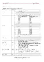
Страница 8: ...cteristics and luminous source charcteristics are not considered 4 4 Image output Format Coyote Application Setting 1 RAW Mode 1 Tap Bayer RGB Area of interest Width 1624 Height 1224 Offset X 0 Offset...

Страница 9: ...1 15000s 15 1 45000s 1 22000s 16 Manual Shutter Refer to Address 009 and 010 White Balance 003 0 THRU 1 3200K 2 Spare 3 Spare 4 Manual White Balance Address 156 157 158 and 159 Trigger Mode 004 0 Norm...

Страница 10: ...Effective Line 019 020 0 407 Set the address 015 data to 001 Address 019 MSB and address 020 LSB makes total 16 bit Effective Line 3 H step Min Data 0 3 H Max Data 407 1224 H Start Position 016 017 Ef...

Страница 11: ...nput 5V Tolerant Trigger Input 9 TTL Out0 LVTTL 3 3V Output LVAL FVAL DVAL SP Exposure Output 10 TTL In0 LVTTL Input 5V Tolerant Trigger Input 11 NC 12 NC TTL In a a 0 3 Trigger Input etc TTL In a a 0...

Страница 12: ...hernet Connector MOD YSJ88DA03C CN HONDA TSUSHIN KOGYO CO LTD LINK Green LED ACT Yellow LED LINK LED Lighting off Unconnected to LAN Lighting on Connected to LAN Blinking Transmitting the data ACT LED...

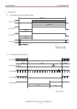
Страница 13: ...Timing LVAL Output 296CLK Video Output DVAL Output 296CLK FVAL Output 1920CLK 1624CLK CLK RAW Mode 64MHz RGB Mode 32MHz 1 CLK 7 2 Full Frame Scan Mode Timing LVAL Output Video Output DVAL Output FVAL...

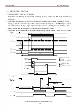
Страница 14: ...utput for the prior signals can not be worked To input trigger signals when the camera is outputting video signals for the prior signals it shall be synchronized with the down edge of camera LVAL outp...

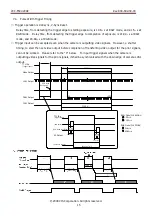
Страница 15: ...shutter timing to start the next video output before completion of transferring video output for the prior signals can not be worked Please refer to the C below To input trigger signals when the came...

Страница 16: ...1221H 3H step Effective line register Address 019 020 0 3H 407 1224H 3H step Total line register Address 021 022 435H Effective line register 2 2 Read Only Note Reading out position and effective line...

Страница 17: ...er data CR 000000 fixed R Read mode Please refer to the address table of Section 5 Function Settings 000 255 0 Dh W Write mode C Camera mode Camera No is fixed with 6 bite numerical strings 000000 Pro...

Страница 18: ...sure to input CR to confirm the end of the command Note When setting the data with 2 Byte High Byte shall be set first then Low Byte to the next The camera rewrites the internal resister when receivi...

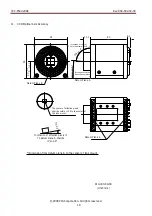
Страница 19: ...optical Axis to datum plane A Datum Plane A 6 3 60 11 1 Datum Plane A 910 003 00 00 Dimension from datum plane A to the center of lens mount The center of effective pixels shall be within 0 6 to the...

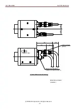
Страница 20: ...6 3 11 1 Product Name Label Position 35 0 1 4 5 0 1 52 GigE DC IN ACT LINK 999 500 00 00 1 2 2 Screw length from C mount lens surface shall be under 6mm And protruding portion shall be lesss than 10mm...

Страница 21: ...F60U29GE Rev 900 682 30 00 2008 CIS Corporation All rights reserved 21 CCXC 12PxxN SONY MOD YSP A1AS SP HONDA TSUSHIN KOGYO Cable Reference Drawing 999 500 00 00 2 2 Unit mm 15 17 51 19 31 23 2 MEGA P...

Страница 22: ...malfunction or non function of the equipment we shall be exempted from responsibility for such damages In case damage or losses are caused by failure to observe the information contained in the instr...

Страница 23: ...th time of usage of the products Cause of the CCD pixel defects is the characteristic phenomenon of CCD itself and CIS is exempted from taking any responsibilities for them Should you have any questio...

Отзывы: