WM8940
Rev 4.4
23
In mixer mode (AUXMODE=1) the on-chip input resistor is bypassed, this allows the user to sum in
multiple inputs with the use of external resistors. When used in this mode there will be gain variations
through this path from part to part due to the variation of the internal 20k
Ω resistors relative to the
higher tolerance external resistors.
REGISTER
ADDRESS
BIT
LABEL
DEFAULT
DESCRIPTION
R1
Power
management 1
6
AUXEN
0
Auxiliary input buffer enable
0 = OFF
1 = ON
R44
Input control
3
AUXMODE
0
0 = inverting buffer
1 = mixer (on-chip input resistor bypassed)
Table 5 Auxiliary Input Buffer Control
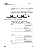
INPUT BOOST
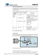
The input BOOST circuit has 3 selectable inputs: the input microphone PGA output, the AUX amplifier
output and the MICP input pin (when not using a differential microphone configuration). These three
inputs can be mixed together and have individual gain boost/adjust as shown in Figure 8.
To ADC input
and output
mixers
AUX2BOOSTVOL=000
MICP2BOOSTVOL=000
Output from
AUX amp
Output from
input PGA
MICP
AUX2BOOSTVOL
R47[2:0]
MICP2BOOSTVOL
R47[6:4]
INPPGAMUTE
R45[6]
PGABOOST
R47[8]
-12dB to + 6dB
-12dB to + 6dB
0dB or +20dB
Figure 8 Input Boost Stage
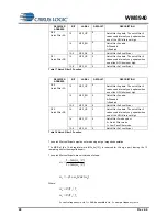
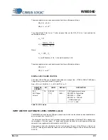
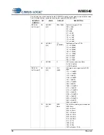
The input PGA path can have a +20dB boost (PGABOOST=1) a 0dB pass through (PGABOOST=0)
or be completely isolated from the input boost circuit (INPPGAMUTE=1).
REGISTER
ADDRESS
BIT
LABEL
DEFAUL
T
DESCRIPTION
R45
Input PGA gain
control
6
INPPGAMUTE
1
Mute control for input PGA:
0=Input PGA not muted, normal operation
1=Input PGA muted (and disconnected from
the following input BOOST stage).
R47
Input BOOST
control
8
PGABOOST
0
0 = PGA output has +0dB gain through input
BOOST stage.
1 = PGA output has +20dB gain through
input BOOST stage.
Table 6 Input BOOST Stage Control


