background image

58

DS726PP2

CS4525

6.2.7

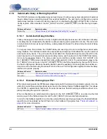
Automatic Power Stage Shut-Down

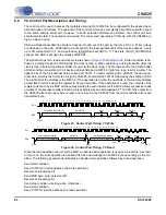
To protect itself from permanent damage, the CS4525 will automatically shut down its internal PWM pow-
er output stages when a thermal error, PWM power output over-current error, or VP under-voltage condi-
tion occurs. In the shut-down state, all digital functions of the device will operate as normal, however the
PWM power output pins become high-impedance.

The levels of the over-current error, thermal error, and VP under-voltage trigger points are listed in the

PWM Power Output Characteristics

 table on 

page 20

. Shut-down will occur automatically whenever the

preset thresholds for thermal error or under-voltage are crossed. 

When the over-current threshold is crossed, the CS4525 will attempt to automatically resume power out-
put operation after an over-current error is encountered and before placing its PWM power outputs in the
shut-down state. Upon the detection of an over-current condition, the CS4525 will place the PWM power
outputs in a high-impedance state, wait approximately 85 ms, and then re-engage the power outputs in
an attempt to resume normal operation. If another over-current condition is immediately detected, the
PWM power outputs will again be placed in a high-impedance state before retrying to resume normal op-
eration a second time. It will continue this sequence for a maximum of five attempts. After the fifth unsuc-
cessful attempt, the outputs will remain in the high-impedance shut-down state.

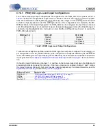
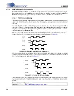
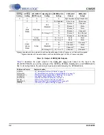
Once in the shut-down state, the RST signal must be toggled low and then high to resume normal device
operation.

6.3

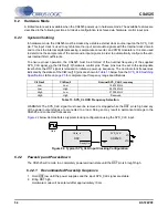
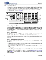
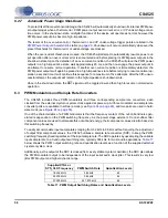
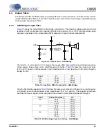
PWM Modulators and Sample Rate Converters

The CS4525 includes three PWM modulators and three corresponding sample rate converters, each
clocked from the external crystal or system clock applied at power-up. All three modulator and sample rate
converter pairs are available in software mode (see 

Figure 14 on page 29

), and two pairs are used in hard-

ware mode (see 

Figure 24 on page 56

).

One of the characteristics of a PWM modulator is that the frequency content of the out-of-band noise gen-
erated is dependent on the PWM switching frequency. As the power stage external LC and snubber filter
component values are used to attenuate this out-of band energy, their component values are also based on
this switching frequency. 

To easily accommodate input sample rates ranging from 32 kHz to 96 kHz without requiring the adjustment
of output filter component values, the CS4525 utilizes a sample rate converter (SRC) to keep the PWM
switching frequency fixed regardless of the input sample rate. The SRC operates by upsampling the variable
input sample rate to a fixed output switching rate, typically 384 kHz for most audio applications. 

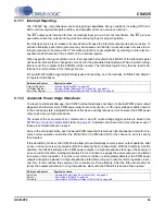
Table 17

below shows the PWM output switching rate and quantization levels as a function of the supplied external
crystal or system clock.

Additionally, as the output of the SRC is clocked from a very stable crystal or oscillator, the SRC also allows
the PWM modulator output to be independent of the input serial audio clock jitter. This results in very low
jitter PWM output and higher dynamic range.

Supplied XTAL or 

SYS_CLK Frequency

PWM Switch Rate

Quantization Levels

18.432 MHz

384 kHz

48

24.576 MHz

384 kHz

64

27.000 MHz

421.875 kHz

64

Table 17. PWM Output Switching Rates and Quantization Levels

Содержание CS4525

Страница 1: ...hannel Digital Serial Port 32 kHz to 96 kHz Input Sample Rates Operation with On Chip Oscillator Driver or Applied SYS_CLK at 18 432 24 576 or 27 000 MHz Integrated Sample Rate Converter SRC Eliminates Clock Jitter Effects Input Sample Rate Independent Operation Simplifies System Integration Spread Spectrum PWM Modulation Reduces EMI Radiated Energy Low Quiescent Current Features continued on page...

Страница 2: ...Desktop Audio General Description The CS4525 is a stereo analog or digital input PWM high efficiency Class D amplifier audio system with an integrated stereo analog to digital A D converter The stereo power amplifiers can deliver up to 15 W per channel into 8 Ω speakers from a small space saving 48 pin QFN package The PWM amplifier can achieve greater than 85 efficiency The package is thermally en...

Страница 3: ... Thermal Limiter 39 6 1 4 12 Thermal Foldback 40 6 1 4 13 2 Way Crossover Sensitivity Control 41 6 1 5 Auxiliary Serial Output 43 6 1 6 Serial Audio Delay Warning Input Port 44 6 1 6 1 Serial Audio Delay Interface 44 6 1 6 2 External Warning Input Port 44 6 1 7 Powered PWM Outputs 45 6 1 7 1 Output Channel Configurations 45 6 1 7 2 PWM Popguard Transient Control 45 6 1 8 Logic Level PWM Outputs 46...

Страница 4: ... 0 69 9 1 4 HP_Detect Mute Pin Active Logic Level HP MutePol 70 9 1 5 HP_Detect Mute Pin Mode HP Mute 70 9 1 6 Modulator Phase Shifting PhaseShift 70 9 1 7 AM Frequency Shifting FreqShift 70 9 2 Input Configuration Address 02h 71 9 2 1 Input Source Selection ADC SP 71 9 2 2 ADC High Pass Filter Enable EnAnHPF 71 9 2 3 Serial Port Sample Rate SPRate 1 0 Read Only 71 9 2 4 Input Serial Port Digital ...

Страница 5: ...nable 2 Way Crossover En2Way 81 9 10 5 2 Way Cross Over Frequency 2WayFreq 2 0 81 9 11 Channel A B 2 Way Sensitivity Control Address 56h 81 9 11 1 Channel A and Channel B Low Pass Sensitivity Adjust LowPass 3 0 81 9 11 2 Channel A and Channel B High Pass Sensitivity Adjust HighPass 3 0 82 9 12 Master Volume Control Address 57h 82 9 12 1 Master Volume Control MVol 7 0 82 9 13 Channel A and B Volume...

Страница 6: ...etected On Channel X OverCurrX 93 9 22 2 External Amplifier State ExtAmpSt 93 9 22 3 Under Voltage Thermal Error State UVTE 1 0 94 9 23 Device I D and Revision Address 63h Read Only 94 9 23 1 Device Identification DeviceID 4 0 94 9 23 2 Device Revision RevID 2 0 94 10 PARAMETER DEFINITIONS 95 11 REFERENCES 95 12 PACKAGE DIMENSIONS 96 13 THERMAL CHARACTERISTICS 97 13 1 Thermal Flag 97 14 ORDERING I...

Страница 7: ...I O Power Rails 12 Table 2 Bass Shelving Filter Corner Frequencies 31 Table 3 Treble Shelving Filter Corner Frequencies 32 Table 4 Bass Management Cross Over Frequencies 35 Table 5 2 Way Cross Over Frequencies 41 Table 6 Auxiliary Serial Port Data Output 43 Table 7 Nominal Switching Frequencies of the Auxiliary Serial Output 43 Table 8 PWM Power Output Configurations 45 Table 9 Typical Ramp Times ...

Страница 8: ... serial audio data HP_DETECT MUTE 7 Headphone Detect Mute Input Headphone detection or mute input signal as configured via the I C control port RST 8 Reset Input The device enters a low power mode and all internal registers are reset to their default settings when this pin is driven low Top Down Through Package View 48 Pin QFN Package 12 7 6 5 4 3 2 1 11 10 9 8 25 30 31 32 33 34 35 36 26 27 28 29 ...

Страница 9: ... Transient Control to suppress the initial pop in half bridge configured outputs VP 25 30 31 36 High Voltage Power Input High voltage power supply for the individual half bridge devices OUT4 OUT3 OUT2 OUT1 26 29 32 35 PWM Output Output Amplified PWM power outputs PWM_SIG2 PWM_SIG1 39 40 Logic Level PWM Output Output Logic Level PWM switching signals DLY_SDOUT 41 Delay Serial Audio Data Out Output ...

Страница 10: ...rial Audio Data Input Input Input for two s complement serial audio data MUTE 7 Mute Input The PWM outputs will output silence as a 50 duty cycle signal when this pin is driven low RST 8 Reset Input The device enters a low power mode and all internal registers are reset to their default settings when this pin is driven low Top Down Through Package View 48 Pin QFN Package 12 7 6 5 4 3 2 1 11 10 9 8...

Страница 11: ... Ramp Capacitor Input This pin should be connected directly to VP in hardware mode VP 25 30 31 36 High Voltage Power Input High voltage power supply for the individual half bridge devices OUT4 OUT3 OUT2 OUT1 26 29 32 35 PWM Output Output Amplified PWM power outputs TSTO 39 40 Test Output Output These pins are outputs used for the Logic Level PWM switching signals available only in software mode Th...

Страница 12: ...5 0 V CMOS 45 AUX_LRCK Output 2 5 V 5 0 V CMOS VD_REG 39 PWM_SIG2 Output 2 5 V CMOS 40 PWM_SIG1 Output 2 5 V CMOS Hardware Mode VD 1 SEL_OSC0 Input 2 5 V 5 0 V 2 SEL_OSC1 Input 2 5 V 5 0 V 3 ADC SP Input 2 5 V 5 0 V 7 MUTE Input 2 5 V 5 0 V 41 TWR Output 2 5 V 5 0 V Open Drain 42 ERRUVTE Output 2 5 V 5 0 V Open Drain 43 ERROC Output 2 5 V 5 0 V Open Drain 44 EN_TFB Input 2 5 V 5 0 V 45 I S LJ Inpu...

Страница 13: ... Output Filter 29 26 PWM_SIG2 39 40 PWM_SIG1 Line Output or Headphone Output Analog Monitor Output Crystal 24 576 MHz XTI XTO 48 47 MPEG Audio Processor or HDMI Receiver SDIN 6 LRCK 4 SCLK 5 46 SYS_CLK 7 HP_DETECT MUTE Lip Synch Delay NJU26902 2 5V VD_REG 11 0 1 µF 10 µF AUX_SCLK 44 DLY_SDOUT 41 DLY_SDIN 42 AUX_LRCK AD0 45 Micro Controller RST 8 INT 1 SDA 3 SCL 2 2 kΩ 22 kΩ 2 kΩ VD AGND 14 VA_REG ...

Страница 14: ...UT2 Output Filter 35 32 OUT3 OUT4 Output Filter 29 26 Analog Monitor Output Audio Processor SDIN 6 LRCK 4 SCLK 5 AGND 14 VA_REG 13 AFILTA 17 AFILTB 18 FILT 15 VQ 16 0 1 µF 10 µF 150 pF 150 pF 10 µF 1 µF LVD 9 VD or GND OCREF 21 16 2 kΩ TSTO TSTI 47 48 46 SYS_CLK Clock 24 576 MHz CLK_FREQ0 1 CLK_FREQ1 2 7 MUTE EN_TFB 44 TWR 41 ERRUVTE 42 I S LJ 45 Micro Controller RST 8 22 kΩ VD 43 ERROC ADC SP 3 V...

Страница 15: ...ut Left Speaker Right Speaker Subwoofer Figure 3 Typical System Configuration 1 Main Tuner A V Switch PIP Tuner A V In 1 A V In 2 A V In X Monitor Out Audio Delay Analog Out Analog In Analog Out 27 MHz Crystal In Crystal Out CS4525 PWM_SIG1 PWM_SIG2 Gate Drive Gate Drive Gate Drive Gate Drive CS4412A PWM In Status Out Subwoofer 2 x 15 W Stereo 1 x 30 W Subwoofer Power Foldback Aux Out Analog In Di...

Страница 16: ... Gate Drive Gate Drive CS4412A PWM In Status Out Gate Drive Gate Drive Gate Drive Gate Drive CS4412A PWM In Status Out Left Speaker Right Speaker Subwoofer 2 x 30 W Stereo 1 x 30 W Subwoofer Power Foldback Aux Out Analog In Digital In Delay Port Gate Drive Gate Drive Gate Drive Gate Drive Clock Out SYS_CLK Control Port Control Port Sound Processor Var Fixed Out 22 kΩ 22 kΩ Figure 5 Typical System ...

Страница 17: ...25 PWM_SIG1 PWM_SIG2 Power Foldback Aux Out Analog In Digital In Delay Port Gate Drive Gate Drive Gate Drive Gate Drive SYS_CLK Control Port CS4525 PWM_SIG1 PWM_SIG2 Power Foldback Aux Out Analog In Digital In Delay Port Gate Drive Gate Drive Gate Drive Gate Drive SYS_CLK Control Port Analog Out Digital Out Monitor Out Var Fixed Out Left Woofer Left Tweeter Right Woofer Right Tweeter Sub Out Figur...

Страница 18: ...tch up 3 The maximum over under voltage is limited by the input current Parameters Symbol Min Nom Max Units DC Power Supply Digital and Analog Core Note 1 VD 2 375 2 5 2 625 V VD 3 135 3 3 3 465 V VD 4 75 5 0 5 25 V Amplifier Outputs VP 8 0 18 0 V Temperature Ambient Temperature Commercial TA 10 70 C Junction Temperature TJ 10 125 C Parameters Symbol Min Max Units DC Power Supply Power Stage Outpu...

Страница 19: ...ing frequency Fs With a 27 000 MHz or 24 576 MHz XTAL SYS_CLK Fs is equal to the applied clock divided by 512 With an 18 432 MHz XTAL SYS_CLK Fs is equal to the applied clock divided by 384 Parameter Min Typ Max Unit Dynamic Range Note 4 A weighted unweighted 90 87 95 92 dB dB Total Harmonic Distortion Noise 1 dB 20 dB 60 dB 86 72 32 77 dB dB dB DC Accuracy Interchannel Gain Mismatch 0 05 dB Gain ...

Страница 20: ...2 7 5 5 30 23 5 W W W W W W Total Harmonic Distortion Noise Stereo Full Bridge Half Bridge Parallel Full Bridge THD N PO 1 W PO 0 dBFS 11 3 W PO 1 W PO 0 dBFS 5 0 W PO 1 W PO 0 dBFS 22 6 W 0 05 0 10 0 12 0 28 0 1 0 3 Dynamic Range Stereo Full Bridge Half Bridge Parallel Full Bridge DYR PO 60 dBFS A Weighted PO 60 dBFS Unweighted PO 60 dBFS A Weighted PO 60 dBFS Unweighted PO 60 dBFS A Weighted PO ...

Страница 21: ...e power supplies and clocks are stable Parameters Symbol Min Nominal Max Units Supported Input Sample Rates FSI 28 5 39 5 39 5 86 4 32 44 1 48 96 35 2 52 8 52 8 105 6 kHz kHz kHz kHz LRCK Duty Cycle 45 55 SCLK Frequency Note 8 Note 9 1 tp FSI 2 Nbits FCLK 3 Hz SCLK Duty Cycle 45 55 LRCK Setup Time Before SCLK Rising Edge ts LK SK 40 ns SDIN Setup Time Before SCLK Rising Edge ts SD SK 25 ns SDIN Ho...

Страница 22: ...O 64 FSO Hz Hz Hz AUX_SCLK Duty Cycle 50 AUX_SCLK Period 1 FSCLKO s Input Source Serial Audio Input Port Output Sample Rate FS In 32kHz 44 1 kHz 48 kHz FS In 96 kHz FSO FSI FSI 2 Hz Hz AUX_LRCK Duty Cycle Note 13 45 55 AUX_LRCK Period Note 12 13 TSI TCLK TSI TSI TCLK s AUX_SCLK Frequency FS In 32kHz 44 1 kHz 48 kHz Note 14 FS In 96 kHz FSCLKI FSCLKI 2 Hz Hz AUX_SCLK Duty Cycle 30 70 AUX_SCLK Perio...

Страница 23: ... 27 000 18 617 24 822 27 270 MHz MHz MHz XTI Duty Cycle 45 50 55 Parameter Symbol Min Typ Max Unit External Clock Operating Frequency ClkFreq 1 0 00 Note 15 ClkFreq 1 0 01 ClkFreq 1 0 10 FCLK 18 240 24 330 26 730 18 432 24 576 27 000 18 617 24 822 27 270 MHz MHz MHz Rising Edge RST to start of SYS_CLK tsclko 1024 tsclki SYS_CLK Period tsclki 37 04 54 25 ns SYS_CLK Duty Cycle 45 50 55 SYS_CLK high ...

Страница 24: ...µs Start Condition Hold Time prior to first clock pulse thdst 4 0 µs Clock Low time tlow 4 7 µs Clock High Time thigh 4 0 µs Setup Time for Repeated Start Condition tsust 4 7 µs SDA Hold Time from SCL Falling Note 16 thdd 10 ns SDA Setup time to SCL Rising tsud 250 ns Rise Time of SCL and SDA trc 1 µs Fall Time SCL and SDA tfc 300 ns Setup Time for Stop Condition tsusp 4 7 µs Acknowledge Delay fro...

Страница 25: ...ters Min Typ Max Units Normal Operation Note 17 Power Supply Current VD 3 3 V 54 mA Power Dissipation VD 3 3 V 180 mW Power Down Mode Note 18 Power Supply Current VD 3 3 V 2 8 mA VD_REG Characteristics Nominal Voltage 2 25 2 5 2 75 V DC current source 3 mA VA_REG Characteristics Nominal Voltage 2 25 2 5 2 75 V DC current source 1 mA VQ Characteristics Nominal Voltage 0 5 VA_REG V Output Impedance ...

Страница 26: ...tal via the ClkFreq 1 0 bits in the Clock Config register These bits must be set to the appropriate value before the PDnAll bit is cleared to initiate a power up sequence See the SYS_CLK Switching Specifications and XTI Switching Specifications tables on page 23 for complete input frequency range specifications WARNING The system clock source must never be removed or stopped while any of the power...

Страница 27: ...mpedance Also the DivSysClk bit allows the frequency of the generated internal clock to be divided by 2 prior to be ing driven out of the SYS_CLK It should be noted that the internal oscillator driver is disabled when the CS4525 is in reset RST is low Any external devices connected to the SYS_CLK output will not receive a clock signal until the CS4525 is taken out of reset If an external crystal i...

Страница 28: ...on causes the device to enter software mode and places it in power down mode 4 If the LVD pin is tied low and VD VD_REG and VA_REG are connected to 2 5 V clear the SelectVD bit in the Power Ctrl register to indicate the 2 5 V VD supply level See section 6 7 on page 63 for de tails 5 If VP is connected to a supply voltage less than or equal to 14 V nominal clear the SelectVP bit in the Foldback Cfg...

Страница 29: ...4 below The signal processing blocks are described in detail in the following sections Referenced Control Register Location ADC SP Input Source Selection ADC SP on page 71 DIF 2 0 Input Serial Port Digital Interface Format DIF 2 0 on page 71 EnAnHPF ADC High Pass Filter Enable EnAnHPF on page 71 Amplifier Out 1 Amplifier Out 2 Amplifier Out 3 Amplifier Out 4 PWM Modulator Output 2 Audio Processing...

Страница 30: ...and right channels The channel mixers are controlled by the LChMix 1 0 and RChMix 1 0 bits in the Mixer Config register To allow stereo operation when a mono mix is configured when the HP_DETECT MUTE pin is configured for headphone detection the HP Mute bit is set the operation of the left channel mixer is affected by the active state of the headphone detection input signal In this configuration w...

Страница 31: ...ther is optimized for 44 1 kHz 48 kHz and 96 kHz sample rates The CS4525 automatically detects the input sample rate and chooses the appropriate filter set to apply The available corner frequencies are shown in tables 2 and 3 below and are configured with the BassFc 1 0 and TrebFc 1 0 bits in the Tone Config register Note that the corner frequency of each filter set scales linearly with the input ...

Страница 32: ...kHz 15 0 kHz 44 1 kHz 4 8 kHz 6 7 kHz 9 6 kHz 14 4 kHz 48 kHz 96 kHz 5 2 kHz 7 3 kHz 10 4 kHz 15 6 kHz Table 3 Treble Shelving Filter Corner Frequencies Referenced Control Register Location EnToneCtrl Tone Control Enable EnToneCtrl on page 77 TrebFc 1 0 Treble Corner Frequency TrebFc 1 0 on page 77 BassFc 1 0 Bass Corner Frequency BassFc 1 0 on page 77 Treble 3 0 Treble Gain Level Treb 3 0 on page...

Страница 33: ... to 3 99996 decimal 7F FF FF hex The binary coefficient values are stored in registers 0Ah 54h Each 24 bit coefficient is split into 3 bytes each of which is mapped to an individually accessible register location See the Register Quick Refer ence section beginning on page 66 for the specific register locations for each coefficient By default all b0 coefficients are set to 1 decimal and all other c...

Страница 34: ... register The adaptive loudness compensation feature is enabled by setting the Loudness bit in the Tone Config register When the loudness feature is enabled it immediately evaluates the effective average volume and applies bass and treble boost accordingly When disabled any treble or bass boost applied due to the loudness feature will be removed Because the adaptive loudness compensation filter op...

Страница 35: ...are available The BassMgr 2 0 bits also allow the bass manager to be disabled When disabled the bass management crossover is bypassed and no signal is presented on the sub channel To allow full range headphone operation when the HP_DETECT MUTE pin is configured for headphone detection the HP Mute bit is set the operation of the bass manager is affected by the active state of the headphone detectio...

Страница 36: ...ignal during a mute condition This selection is achieved via the Mute50 50 bit in the Volume Cfg register The AutoMute bit in the same register dictates whether the device will automatically mute after the recep tion of 8192 consecutive samples of static 0 or 1 When the AutoMute function is enabled a single sample of non static data will cause the automatic mute to be released The CS4525 implement...

Страница 37: ...ample rate Fs Recommended settings Best limiting performance may be realized with the fastest attack and slowest release setting with soft ramp enabled in the control registers Use the minimum bits to set a threshold slightly below the maximum threshold to cushion the sound as the limiter attacks and releases By default the limiter affects all channels when the maximum threshold is exceeded on any...

Страница 38: ...can be enabled by setting the EnLimiter bit in the Limiter Cfg 1 register The limiter can also be used in conjunction with the thermal limiter function to provide thermal error pro tection to the CS4525 The thermal limiter function is described in Thermal Limiter on page 39 Referenced Control Register Location EnLimiter Peak Detect and Limiter Enable EnLimiter on page 86 LimitAll Peak Signal Limit...

Страница 39: ...If the thermal limiter is engaged and the peak signal limiter is dis abled via the EnLimiter bit the peak signal limiter will be automatically enabled and its minimum and maximum thresholds will be set to 3 dB If the thermal limiter is engaged and the peak signal limiter is enabled an additional 3dB will be automatically applied to the minimum and maximum thresholds estab lished in the Limiter Cfg...

Страница 40: ... power capability Attenuation applied due to thermal foldback reduces the audio output level in a linear manner Figure 18 below demonstrates the foldback process Thermal Warning Threshold tdelay 1 2 2 2 2 3 1 Foldback Attack Delay AttackDly 1 0 tdelay tdelay tdelay tdelay 3 The junction temperature is checked once again after the next foldback attack timer timeout If it has remained below the ther...

Страница 41: ...l Warning Input Port on page 44 for more information 6 1 4 13 2 Way Crossover Sensitivity Control The CS4525 implements a dedicated stereo 24 dB octave Linkwitz Riley crossover filter with adjustable cross over frequency and sensitivity control to facilitate 2 way speaker configurations The filter s high pass output can be used to drive the tweeter and its low pass output is used can be drive the ...

Страница 42: ...y of both channel A and channel B high and low pass outputs The 2 way crossover can be enabled by setting the En2Way bit in the Volume Cfg register X Over Freq 5 3 0 kHz 2 88 kHz 3 13 kHz X Over Freq 6 3 2 kHz 3 07 kHz 3 34 kHz X Over Freq 7 3 4 kHz 3 26 kHz 3 55 kHz Referenced Control Register Location En2Way Enable 2 Way Crossover En2Way on page 81 2WayFreq 2 0 2 Way Cross Over Frequency 2WayFre...

Страница 43: ..._LRCK AUX_SCLK and AUX_SDOUT pins continuously drive a logic 0 It should be noted that when the CS4525 is configured for analog input the AUX_LRCK AUX_SCLK and AUX_SDOUT pins will contin uously drive a logic 0 if either the PDnADC bit or PDnAll bit is set LChDSel 1 0 Aux Left Channel Data RChDSel 1 0 Aux Right Channel Data 00 Channel A 00 Channel A 01 Channel B 01 Channel B 10 Sub Channel 10 Sub C...

Страница 44: ...cked from AUX_LRCK and AUX_SCLK The serial data is output on the DLY_SDOUT pin and input on the DLY_SDIN EX_TWR in the format specified by the AuxI S LJ bits in the Aux Config register Because the delay interface uses the auxiliary port clock signals the auxiliary se rial port must be enabled using the EnAuxPort bit in the Aux Port Configuration register to allow the delay interface to operate pro...

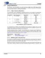
Страница 45: ...r is enabled channel 1 and 2 contain the 2 way crossover channel A high and low pass outputs respectively For more information see the Digital Sound Processing section and Figure 14 on page 29 6 1 7 2 PWM Popguard Transient Control The CS4525 uses Popguard technology to minimize the effects of power up and power down output tran sients commonly produced by half bridge single supply amplifiers impl...

Страница 46: ... input to an external PWM amplifier such as the CS4412 or as an analog input to a headphone amplifier or a line out amplifier To eliminate power up pops when used to supply an external PWM amplifier the CS4525 implements the same click free start up function on the PWM_SIG outputs as it does for its own powered PWM outputs This function can only be utilized if the PWM amplifier has an initial tran...

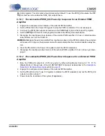
Страница 47: ...ING Releasing the external amplifier from reset power down before PWM modulators have started will cause a DC output on the speakers unless the external amplifier has an initial transition delay fea ture 6 Clear the PDnAll bit in the Power Ctrl register to start the PWM modulators 7 Disengage the reset power down feature of the external PWM amplifier if it has not been yet disen gaged 6 1 8 2 Reco...

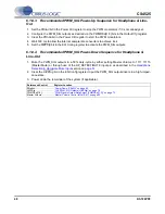
Страница 48: ...uts 6 1 8 4 Recommended PWM_SIG Power Down Sequence for Headphone Line Out 1 Mute the PWM_SIG outputs to a 50 duty cycle by either setting Master Volume to 1111 1111h Master Mute or through use of the HP_DETECT MUTE input pin as described in the Headphone Detection Hardware Mute Input section on page 51 2 Clear the HiZPSig bit in the EQ Config register to put the PWM_SIG output drivers in a high i...

Страница 49: ...ut configuration if the HP_DETECT MUTE pin is configured for headphone detection the HP Mute bit is set the PWM logic level output mapping can be affected by the active state of the headphone detection input signal See the Headphone Detection Hardware Mute Input section on page 51 for more informa tion It should be noted that signal on channels 1 2 and the sub channel are dependent upon the digita...

Страница 50: ...ltiplying the setting of the OutputDly 3 0 bits by the period of the input clock source By default no delay is inserted When the power outputs are configured for 2 channel full bridge operation the OUT3 OUT4 signal pair is delayed from the OUT1 OUT2 signal pair by the delay amount as shown in Figure 20 When the power outputs are configured for 3 channel 2 channel half bridge and 1 channel full bri...

Страница 51: ...e When configured as a headphone detect input pin and the HP_DETECT MUTE input is active the PWM_SIG1 and PWM_SIG2 output pins can output audio from channel 1 and channel 2 respectively re gardless of the setting of the PWMDSel 1 0 bits The OUT1 OUT4 PWM driver outputs will mute by out putting a non modulated 50 duty cycle signal While the headphone detect input signal is active the channel mixing...

Страница 52: ...l 2 Sub Channel Active X 01 10 or 11 Mute Mute 1 Head phone Mode Not Active X 01 10 or 11 Mute Mute Active 000 Disabled 01 Channel 1 Channel 2 10 Channel 1 Mute 11 Channel 2 Mute 001 through 111 01 10 or 11 Channel 1 Channel 2 Signals denoted with one asterisk do not have Bass Manager 2 Way Crossover or Channel Mix applied Signals denoted with two asterisks do not have Bass Manager or 2 Way Crosso...

Страница 53: ... of the device will operate as normal however the PWM power output pins become high impedance The levels of the over current error thermal error and VP under voltage trigger points are listed in the PWM Power Output Characteristics table on page 20 Automatic shut down will occur whenever any of these preset thresholds are crossed Once in the shut down state each powered PWM outputs will remain as ...

Страница 54: ...eased to initiate a power up sequence The nominal clock frequencies indicated by the states of the ClkFreq 1 0 pins are shown in Table 13 below See the SYS_CLK Switching Specifications table on page 23 for complete input frequency range specifications WARNING The SYS_CLK signal must never be removed or stopped while the RST pin is high and any of the power output stages are connected to a load Doi...

Страница 55: ...us ing any audible pops or clicks In hardware mode the serial audio input port supports both I S and left justified formats The serial audio interface format is selected by the I2S LJ pin as shown in Table 15 below 6 2 4 PWM Channel Delay In hardware mode the CS4525 offsets the PWM switching edges between channels as a method of man aging switching noise and reducing radiated emissions The OUT3 OU...

Страница 56: ...ero crossing detection features are active in hard ware mode 6 2 5 3 Warning and Error Reporting The CS4525 is capable of reporting various error and warning conditions on its TWR ERROC and ER RUVTE pins The TWR pin indicates the presence of a thermal warning condition When active concurrently with the ERRUVTE pin indicates a thermal error condition The ERROC pin indicates the presence of an over ...

Страница 57: ...ed Thermal Foldback Enable State Low Thermal foldback disabled High Thermal foldback enabled Table 16 Thermal Foldback Enable Selection Thermal Warning Threshold tdelay 1 2 2 2 2 3 1 Foldback Attack Delay Approximately 2 sec tdelay tdelay tdelay tdelay 1 When the junction temperature crosses the thermal warning threshold the foldback attack delay timer is started 2 When the foldback attack delay t...

Страница 58: ...sume normal device operation 6 3 PWM Modulators and Sample Rate Converters The CS4525 includes three PWM modulators and three corresponding sample rate converters each clocked from the external crystal or system clock applied at power up All three modulator and sample rate converter pairs are available in software mode see Figure 14 on page 29 and two pairs are used in hard ware mode see Figure 24...

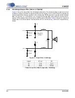
Страница 59: ...peaker these values set the cutoff frequency of the filter Table 18 shows the component values for L1 and C1 based on nominal speaker load impedance for a corner frequency 3 dB point of approx imately 35 kHz C2 is the DC blocking capacitor Table 19 shows the component values for C2 based on corner frequency 3 dB point and a nominal speaker load impedances of 4 Ω 6 Ω and 8 Ω This capacitor should a...

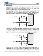
Страница 60: ...y reduce radiated EMI The inductors L1 and capacitor C1 comprise the low pass filter Along with the nominal load im pedance of the speaker these values set the cutoff frequency of the filter Table 20 shows the component values based on nominal speaker load impedance for a corner frequency 3 dB point of approximately 35 kHz Load L1 L2 C1 4 Ω 10 µH 1 0 µF 6 Ω 15 µH 0 47 µF 8 Ω 22 µH 0 47 µF Table 20...

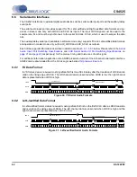
Страница 61: ...ows the recommended input circuit for 2 VRMS inputs It includes a 8 4 dB passive attenuator to condition the input signal for the CS4525 s full scale input voltage a first order passive low pass filter that has less than 0 05 dB of attenuation at 24 kHz and a DC blocking capacitor to accommodate for the analog input pins bias level The passive attenuator network should be placed as close as possib...

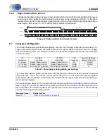
Страница 62: ...22 respectively for the precise timing and tolerances of each signal For additional information application note AN282 presents a tutorial of the 2 channel serial audio interface AN282 can be downloaded from the Cirrus Logic web site at http www cirrus com 6 6 1 I S Data Format In I S format data is received most significant bit first one SCLK delay after the transition of LRCK and is valid on the...

Страница 63: ...ominal output voltage of 2 5 V The output of the analog regulator is presented on the VA_REG pin and must only be connected to the bypass capacitors as shown in the typ ical connection diagrams If a nominal supply voltage of 2 5 V is used as the VD supply see the Recommended Operating Conditions table on page 18 the VD VD_REG and VA_REG pins must all be connected to the VD supply source In this co...

Страница 64: ... the setting of AD0 The eighth bit of the address is the R W bit If the operation is a write the next byte is the memory address pointer MAP which selects the register to be read or written If the operation is a read the contents of the register pointed to by the MAP will be output Setting the auto increment bit in MAP allows successive reads or writes of consecutive registers Each byte is separat...

Страница 65: ...4525 to minimize inductance effects All signals especially clocks should be kept away from the FILT and VQ pins in order to avoid unwanted coupling into the modulators The FILT and VQ decoupling capacitors particularly the 0 1 µF must be positioned to minimize the electrical path from FILT and AGND The CRD4525 reference design demonstrates the optimum layout and power sup ply arrangements 7 2 QFN ...

Страница 66: ...e1 PreScale0 Reserved RChMix1 RChMix0 LChMix1 LChMix0 page 75 0 0 0 0 0 0 0 0 07h Tone Config DeEmph Loudness EnDigHPF TrebFc1 TrebFc0 BassFc1 BassFc0 EnToneCtrl page 76 0 0 0 0 0 0 1 0 08h Tone Control Treble3 Treble2 Treble1 Treble0 Bass3 Bass2 Bass1 Bass0 page 78 1 0 0 0 1 0 0 0 09h EQ Config Freeze HiZPSig BassMgr2 BassMgr1 BassMgr0 Reserved EnChBPEq EnChAPEq page 78 0 0 0 0 0 0 0 0 0Ah BiQuad...

Страница 67: ...MSB 7 38h MSB 8 LSB 8 39h LSB 7 LSB 3Ah BiQuad 4 A2 Coeff MSB MSB 7 3Bh MSB 8 LSB 8 3Ch LSB 7 LSB 3Dh BiQuad 4 B0 Coeff MSB MSB 7 3Eh MSB 8 LSB 8 3Fh LSB 7 LSB 40h BiQuad 4 B1 Coeff MSB MSB 7 41h MSB 8 LSB 8 42h LSB 7 LSB 43h BiQuad 4 B2 Coeff MSB MSB 7 44h MSB 8 LSB 8 45h LSB 7 LSB 46h BiQuad 5 A1 Coeff MSB MSB 7 47h MSB 8 LSB 8 48h LSB 7 LSB 49h BiQuad 5 A2 Coeff MSB MSB 7 4Ah MSB 8 LSB 8 4Bh LS...

Страница 68: ...MuteChB MuteChA page 84 0 0 0 0 0 0 0 0 5Ch Limiter Cfg 1 Max2 Max1 Max0 Min2 Min1 Min0 LimitAll EnLimiter page 85 0 0 0 0 0 0 1 0 5Dh Limiter Cfg 2 Reserved Reserved RRate5 RRate4 RRate3 RRate2 RRate1 RRate0 page 87 0 0 1 1 1 1 1 1 5Eh Limiter Cfg 3 EnThLim Reserved ARate5 ARate4 ARate3 ARate2 ARate1 ARate0 page 87 0 0 0 0 0 0 0 0 5Fh Power Ctrl AutoRetry EnOCProt SelectVD PDnADC PDnOut3 4 PDnOut...

Страница 69: ...is divider is only available if the clock source is an external crystal attached to XTI XTO and the SYS_CLK output is enabled 9 1 3 Clock Frequency ClkFreq 1 0 Default 01 Function These bits must be set to identify the nominal clock frequency of the crystal attached to the XTI XTO pins or that of the input SYS_CLK signal See the XTI Switching Specifications table on page 23 and the SYS_CLK Switchi...

Страница 70: ... shifted by 180 degrees This causes for instance the differential sig nal pair to be exactly in phase with one another during a mute condition thereby reducing the amount of switching current through the load 9 1 7 AM Frequency Shifting FreqShift Default 0 Function Controls the state of the PWM AM frequency shift feature See PWM AM Frequency Shift on page 51 for more information HP MutePol Setting...

Страница 71: ...data in on SDIN The required relationship between the Left Right clock serial clock and serial data is defined by the Digital Interface Format and the options are detailed in the section Serial Audio Interfaces on page 62 7 6 5 4 3 2 1 0 ADC SP EnAnHPF Reserved SPRate1 SPRate0 DIF2 DIF1 DIF0 ADC SP Setting Audio Input Source 0 Digital input from the serial audio input port 1 Analog input from the ...

Страница 72: ...d in the Serial Audio Interfaces on page 62 9 3 4 Aux Serial Port Right Channel Data Select RChDSel 1 0 Default 01 Function Selects the data to be sent over the right channel of the auxiliary port serial data output signal 7 6 5 4 3 2 1 0 EnAuxPort DlyPortCfg1 DlyPortCfg0 AuxI S LJ RChDSel1 RChDSel0 LChDSel1 LChDSel0 EnAuxPort Setting Auxiliary Port State 0 Auxiliary port disabled 1 Auxiliary port...

Страница 73: ...s OutputDly 3 0 Default 0000 Function The channel delay bits allow delay adjustment of each of the power output audio channels The value of this register determines the amount of delay inserted in the output path The delay time is calculated by multiplying the register value by the period of the SYS_CLK or crystal input clock source These bits can LChDSel 1 0 Setting Aux Serial Port Left Channel O...

Страница 74: ...r than 14 V 9 5 2 Enable Thermal Foldback EnTherm Default 0 Function Enables the thermal foldback feature See Thermal Foldback on page 40 for more information 9 5 3 Lock Foldback Adjust LockAdj Default 0 Function Controls the operation of the foldback lock adjustment feature See Thermal Foldback on page 40 for more information OutputDly 3 0 Setting Output Delay in Input Clock Source Cycles 0000 0 ...

Страница 75: ...tenuation PreScale 2 0 Default 000 Function Controls the pre scale attenuation level See Pre Scaler on page 30 for more information AttackDly 1 0 Setting Foldback Attack Time 00 Approximately 0 5 seconds 01 Approximately 1 0 seconds 10 Approximately 1 5 seconds 11 Approximately 2 0 seconds EnFloor Setting Attenuation Floor 0 No foldback attenuation floor imposed 1 Maximum foldback attenuation limi...

Страница 76: ...ntrol Loudness Default 0 Function Controls the operation of the adaptive loudness compensation feature See Adaptive Loudness Compen sation on page 34 for more information RChMix 1 0 Setting Right Channel Mixer Output on Channel B 00 Right Channel 01 Left Channel Right Channel 2 10 Left Channel Right Channel 2 11 Left Channel LChMix 1 0 Setting Left Channel Mixer Output on Channel A 00 Left Channel...

Страница 77: ...helving filters When cleared disables the bass and treble shelv ing filters EnDigHPF Setting Digital Signal Processing High Pass Filter State 0 Digital signal processing high pass filter disabled 1 Digital signal processing high pass filter enabled TrebFc 1 0 Setting Treble Corner Frequency 00 Selects Treble Fc 0 Approximately 5 kHz 01 Selects Treble Fc 1 Approximately 7 kHz 10 Selects Treble Fc 2...

Страница 78: ...s 57h channel X volume control address 58h 5Ah and bi quad coefficient registers for channel A and channel B address 0Ah 54h without the changes taking effect until the Freeze bit is disabled To make multiple changes in these control port registers take effect simultaneously enable the Freeze bit make all register changes then disable the Freeze bit 7 6 5 4 3 2 1 0 Treble3 Treble2 Treble1 Treble0 ...

Страница 79: ... for channel B 9 9 5 Enable Channel A Parametric EQ EnChAPEq Default 0 Function Enables the parametric EQ bi quad filters for channel A HiZPSig Setting PWM_SIG Output Driver State 0 High impedance 1 Drivers active BassMgr 2 0 Setting Bass Manager Crossover Setting 000 Bass manager disabled 001 Selects Bass Manager Frequency 1 Approximately 80 Hz 010 Selects Bass Manager Frequency 2 Approximately 1...

Страница 80: ...changes both muting and attenuation will occur on a signal zero crossing to minimize audible artifacts The requested level change will occur after a timeout period approximately 18 7 ms for a PWM switch rate of 384 768 kHz and 17 0 ms for a PWM switch rate of 421 875 843 75 kHz if the signal does not encounter a zero crossing The zero cross function is independently monitored and implemented for e...

Страница 81: ...re information En2Way Setting 2 Way Crossover State 0 2 way crossover disabled 1 2 way crossover enabled 2WayFreq Setting 2 Way Crossover Frequency 000 Selects X Over Freq 0 Approximately 2 0 kHz 001 Selects X Over Freq 1 Approximately 2 2 kHz 010 Selects X Over Freq 2 Approximately 2 4 kHz 011 Selects X Over Freq 3 Approximately 2 6 kHz 100 Selects X Over Freq 4 Approximately 2 8 kHz 101 Selects ...

Страница 82: ... Control MVol 7 0 Default 2Ah Function Sets the gain attenuation level of the master volume control See Volume and Muting Control on page 36 for more information HighPass 3 0 Setting Sensitivity Compensation Level 0000 0 0 dB 0001 0 5 dB 0010 1 0 dB 1000 4 0 dB 1110 7 0 dB 1111 7 5 dB 7 6 5 4 3 2 1 0 MVol7 MVol6 MVol5 MVol4 MVol3 MVol2 MVol1 MVol0 MVol 7 0 Setting Master Volume Setting 0000 0000 2...

Страница 83: ...he gain attenuation levels of the sub channel See Volume and Muting Control on page 36 for more information 7 6 5 4 3 2 1 0 ChXVol7 ChXVol6 ChXVol5 ChXVol4 ChXVol3 ChXVol2 ChXVol1 ChXVol0 ChXVol 7 0 Setting Channel X Volume Setting 0000 0000 24 dB 0011 0000 0 0 dB 0011 0001 0 5 dB 0011 0010 1 0 dB 1111 1110 103 0 dB 1111 1111 Channel Mute 7 6 5 4 3 2 1 0 SubVol7 SubVol6 SubVol5 SubVol4 SubVol3 Sub...

Страница 84: ...lt 0 Function The output of the ADC will mute when enabled 9 15 5 Independent Channel A B Mute MuteChX Default 0 Function The respective channel s power PWM logic level PWM and auxiliary serial data outputs will enter a mute state when enabled The delay serial output will be unaffected if the delay port is enabled The muting 7 6 5 4 3 2 1 0 InvADC InvSub InvCh2 InvCh1 MuteADC MuteSub MuteChB MuteC...

Страница 85: ...e maximum level below full scale at which to limit and attenuate the output signal at the limiter attack rate 9 16 2 Minimum Threshold Min 2 0 Default 000 Function Sets a minimum level below full scale at which the limiter will begin to release its applied attenuation MuteChX Setting Channel X PWM Mute State 0 Channel X PWM outputs un muted 1 Channel X PWM outputs muted MuteSub Setting Sub Channel...

Страница 86: ...in response to any single channel indicating clipping See Peak Signal Limiter on page 37 for more information 9 16 4 Peak Detect and Limiter Enable EnLimiter Default 0 Function Limits the maximum signal amplitude to prevent clipping when this function is enabled Peak signal limit ing is performed by digital attenuation LimitAll Setting Limit All Channels Configuration 0 Only individual channels af...

Страница 87: ... a thermal warning is detected after the thermal limiter function has been enabled For more details see the Thermal Limiter section on page 39 9 18 2 Limiter Attack Rate ARate 5 0 Default 000000 Function Sets the rate at which the limiter attenuates the analog output from levels above the maximum setting in the limiter threshold register The limiter attack rate is a function of the sampling freque...

Страница 88: ...lects between a VD of 2 5 V 3 3 V or 5 0 V 9 19 4 Power Down ADC PDnADC Default 1 Function The ADC will enter a power down state when this bit is enabled 9 19 5 Power Down PWM Power Output X PDnOutX Default 1 Function When set the specific PWM power output will enter a power down state Only the output power stage is powered down The PWM modulator is not affected nor is the setup or delay register ...

Страница 89: ...rol registers are retained in this state Once the PDnAll bit is disabled the pow ered and logic level PWM outputs will first perform a click free start up function and then resume normal operation The PDnAll bit defaults to enabled on power up and must be disabled before normal operation can occur 9 20 Interrupt Address 60h Bits 7 4 in this register are read only A 1 b in these bit positions indic...

Страница 90: ...e as appropriate since the last read of this register This interrupt bit is an edge triggered event and will be cleared following a read of this register If this bit is set indicating a channel over range condition and the ChOvflM bit is set the INT pin will go active To determine the current overflow state of each channel read the ChXOvflSt and SubOvflSt bits in the interrupt status register 9 20...

Страница 91: ...DCOvfl condition is masked meaning that its occurrence will not affect the INT pin However the ADCOvfl and ADCOvflSt bits will continue to reflect the overflow state of the ADC 9 20 7 Mask for Channel X and Sub Overflow ChOvflM Default 0 Function This bit serves as a mask for the channel 1 2 and Sub overflow interrupt source If this bit is set the ChO vfl interrupt is unmasked meaning that if the ...

Страница 92: ...icates the SRC is currently locked When cleared indicates the SRC is currently unlocked 9 21 2 ADC Overflow ADCOvflSt Function This bit is read only and will identify the presence of an overflow condition within the ADC When set in dicates that an over range condition is currently occurring in the CS4525 ADC signal path and has been clipped to positive or negative full scale 9 21 3 Sub Overflow Su...

Страница 93: ...ondition is currently present on the corresponding amplifier output 9 22 2 External Amplifier State ExtAmpSt Function When set indicates a thermal warning condition is currently being reported by an external amplifier For proper operation the delay serial port must be configured to support an external thermal warning input signal This status bit reflects the active state of the external thermal wa...

Страница 94: ... 11111 Function Identification code for the CS4525 9 23 2 Device Revision RevID 2 0 Function Identifies the CS4525 device revision UVTE 1 0 Setting Under Voltage Thermal Error Status 00 The device is operating normally 01 The device is operating normally however a Thermal Warning condition is being reported 10 An Under Voltage condition is currently present 11 A Thermal Error condition is currentl...

Страница 95: ... The 0 dB reference point is 1 kHz The amplitude cor ner Ac lists the maximum deviation in amplitude above and below the 1 kHz reference point The listed minimum and maximum frequencies are guaranteed to be within the Ac from minimum frequency to maxi mum frequency inclusive Interchannel Isolation A measure of crosstalk between the left and right channels Measured for each channel at the converter...

Страница 96: ...X MIN NOM MAX A 0 0354 0 90 1 A1 0 0000 0 0020 0 00 0 05 1 b 0 0118 0 0138 0 0157 0 30 0 35 0 40 1 2 D 0 3543 BSC 9 00 BSC 1 D2 0 2618 0 2677 0 2736 6 65 6 80 6 95 1 E 0 3543 BSC 9 00 BSC 1 E2 0 2618 0 2677 0 2736 6 65 6 80 6 95 1 e 0 0256 BSC 0 65 BSC 1 L 0 0177 0 0217 0 0276 0 45 0 55 0 70 1 JEDEC MO 220 Controlling Dimension is Millimeters Table 22 Side View A1 Bottom View Top View A Pin 1 ID D...

Страница 97: ...n capability required of the metal plane for a given output power can be calculated as follows θCA TJ MAX TA PD θJC where θCA Thermal resistance of the metal plane in C Watt TJ MAX Maximum rated operating junction temperature in C equal to 150 C TA Ambient temperature in C PD RMS power dissipation of the device equal to 0 15 PRMS assuming 85 efficiency θJC Junction to case thermal resistance of th...

Страница 98: ... parties This document is the property of Cirrus and by furnishing this information Cirrus grants no license express or implied under any patents mask work rights copyrights trademarks trade secrets or other intellectual property rights Cirrus owns the copyrights associated with the information contained herein and gives consent for copies to be made of the information only for use within your org...

Отзывы: