background image

CS2200-CP

DS759F3

17

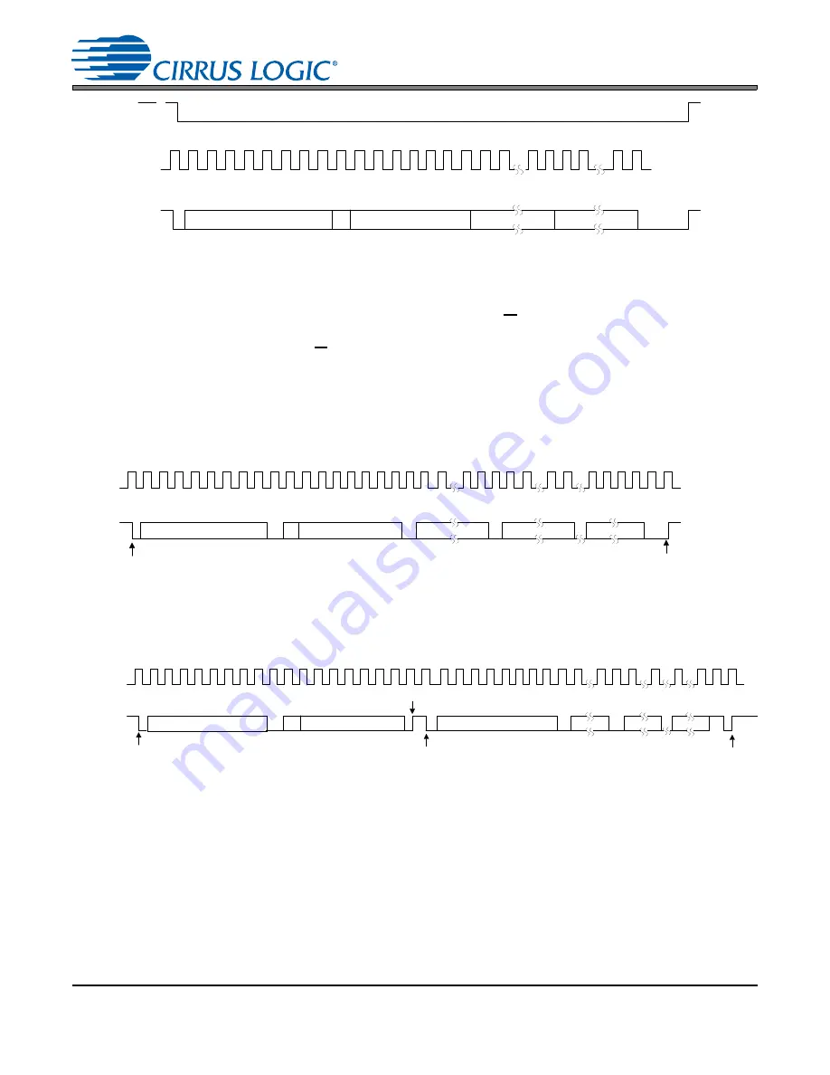
The signal timings for a read and write cycle are shown in 

Figure 12

 and 

Figure 13

. A Start condition is de-

fined as a falling transition of SDA while the clock is high. A Stop condition is a rising transition while the
clock is high. All other transitions of SDA occur while the clock is low. The first byte sent to the 

CS2200

 after

a Start condition consists of the 7-bit chip address field and a R/W bit (high for a read, low for a write). The
upper 6 bits of the 7-bit address field are fixed at 100111 followed by the logic state of the AD0 pin. The
eighth bit of the address is the R/W bit. If the operation is a write, the next byte is the Memory Address Point-
er (MAP) which selects the register to be read or written. If the operation is a read, the contents of the reg-
ister pointed to by the MAP will be output. Setting the auto increment bit in MAP allows successive reads or
writes of consecutive registers. Each byte is separated by an acknowledge bit. The ACK bit is output from
the 

CS2200

 after each input byte is read and is input from the microcontroller after each transmitted byte.

Since the read operation cannot set the MAP, an aborted write operation is used as a preamble. As shown
in 

Figure 12

, the write operation is aborted after the acknowledge for the MAP byte by sending a stop con-

dition. The following pseudocode illustrates an aborted write operation followed by a read operation.

Send start condition. 

Send 100111x0 (chip address & write operation). 

Receive acknowledge bit. 

Send MAP byte, auto increment off. 

Receive acknowledge bit.

4     5     6     7   

CCLK

CHIP ADDRESS

MAP BYTE

DATA

1     0     0      1    1     1     1     0   

CDIN

INCR

   6     5    4     3    2    1    0    7     6         1    0

 0     1     2     3   

8     9   

12   

16   17  

10   11   

13   14  15   

DATA +n     

CS

7     6         1    0

Figure 11.  Control Port Timing in SPI Mode

4     5     6     7   

24  25

SCL

CHIP ADDRESS (WRITE)

MAP BYTE

DATA

DATA +1     

START

ACK

STOP

ACK

ACK

ACK

1     0    0    1    1     1    AD0     0   

SDA

INCR

   6     5    4     3    2    1    0   

7     6         1    0

7     6         1    0

7    6     1    0

 0     1     2     3   

8     9   

12   

16   17  18    19   

10   11   

13   14  15   

27   28

26

DATA +n     

Figure 12.  Control Port Timing, I²C Write

SCL

CHIP ADDRESS (WRITE)

MAP BYTE

DATA

DATA +1

START

ACK

STOP

ACK

ACK

ACK

1     0    0     1    1   1   AD0   0   

SDA

1     0    0     1    1    1   AD0   1   

CHIP ADDRESS (READ)

START

INCR

   6      5     4     3    2    1    0   

7         0

7         0

7         0

NO

16   

8     9   

12   13   14   15   

4     5     6     7   

  0     1   

20   21   22   23   24   

26   27   28   

2     3   

10   11   

17   18    19   

25   

ACK

DATA + n

STOP

Figure 13.  Control Port Timing, I²C Aborted Write + Read

Содержание CS2200-CP

Страница 1: ... a programmable phase lock loop The CS2200 CP is based on an analog PLL architec ture comprised of a Delta Sigma Fractional N Frequency Synthesizer This architecture allows for fre quency synthesis and clock generation from a stable reference clock The CS2200 CP supports both I C and SPI for full soft ware control The CS2200 CP is available in a 10 pin MSOP package in Commercial 10 C to 70 C and A...

Страница 2: ...5 5 5 1 Output Switching 15 5 5 2 PLL Unlock Conditions 15 5 6 Required Power Up Sequencing 16 6 SPI I C CONTROL PORT 16 6 1 SPI Control 16 6 2 I C Control 16 6 3 Memory Address Pointer 18 6 3 1 Map Auto Increment 18 7 REGISTER QUICK REFERENCE 18 8 REGISTER DESCRIPTIONS 19 8 1 Device I D and Revision Address 01h 19 8 1 1 Device Identification Device 4 0 Read Only 19 8 1 2 Device Revision Revision ...

Страница 3: ... 3 Control Port Timing SPI Format Write Only 9 Figure 4 Delta Sigma Fractional N Frequency Synthesizer 10 Figure 5 Internal Timing Reference Clock Divider 11 Figure 6 REF_CLK Frequency vs a Fixed CLK_OUT 11 Figure 7 External Component Requirements for Crystal Circuit 12 Figure 8 Ratio Feature Summary 14 Figure 9 PLL Clock Output Options 14 Figure 10 Auxiliary Output Selection 15 Figure 11 Control ...

Страница 4: ...ctions XTI XTO Timing Reference Clock Input REF_CLK Input Output XTI XTO are I O pins for an external crystal which may be used to generate the low jitter PLL input clock REF_CLK is an input for an externally generated low jitter reference clock AD0 CS 8 Address Bit 0 I C Control Port Chip Select SPI Input AD0 is a chip address pin in I C Mode CS is the chip select signal in SPI Mode SCL CCLK 9 Co...

Страница 5: ... 1 µF VD 3 3 V Notes 1 Resistors required for I2 C operation 2 k AD0 CS Low Jitter Timing Reference System MicroController 1 µF Note1 1 or 2 REF_CLK XTO XTI XTO or 40 pF x 40 pF Crystal To circuitry which requires a low jitter clock N C To other circuitry or Microcontroller Figure 1 Typical Connection Diagram CS2200 CP ...

Страница 6: ...mercial Grade TA 40 C to 85 C Automotive D Grade TA 40 C to 105 C Automotive E Grade Notes 3 To calculate the additional current consumption due to loading per output pin multiply clock output frequency by load capacitance and power supply voltage For example fCLK_OUT 49 152 MHz CL 15 pF VD 3 3 V 2 4 mA of additional current due to these loading conditions on CLK_OUT Parameters Symbol Min Typ Max ...

Страница 7: ...frequency accuracy of the reference clock Parameters Symbol Conditions Min Typ Max Units Crystal Frequency Fundamental Mode XTAL fXTAL RefClkDiv 1 0 10 RefClkDiv 1 0 01 RefClkDiv 1 0 00 8 16 32 14 28 50 MHz MHz MHz Reference Clock Input Frequency fREF_CLK RefClkDiv 1 0 10 RefClkDiv 1 0 01 RefClkDiv 1 0 00 8 16 32 14 28 56 MHz MHz MHz Reference Clock Input Duty Cycle DREF_CLK 45 55 Internal System ...

Страница 8: ...ock Low Time tlow 4 7 µs Clock High Time thigh 4 0 µs Setup Time for Repeated Start Condition tsust 4 7 µs SDA Hold Time from SCL Falling Note 10 thdd 0 µs SDA Setup Time to SCL Rising tsud 250 ns Rise Time of SCL and SDA tr 1 µs Fall Time SCL and SDA tf 300 ns Setup Time for Stop Condition tsusp 4 7 µs Acknowledge Delay from SCL Falling tack 300 1000 ns Delay from Supply Voltage Stable to Control...

Страница 9: ...quency fccllk 6 MHz CCLK Edge to CS Falling Note 11 tspi 500 ns CS High Time Between Transmissions tcsh 1 0 µs CS Falling to CCLK Edge tcss 20 ns CCLK Low Time tscl 66 ns CCLK High Time tsch 66 ns CDIN to CCLK Rising Setup Time tdsu 40 ns CCLK Rising to DATA Hold Time Note 12 tdh 15 ns Rise Time of CCLK and CDIN Note 13 tr2 100 ns Fall Time of CCLK and CDIN Note 13 tf2 100 ns Delay from Supply Vol...

Страница 10: ...lled oscillator VCO The phase comparator compares the fraction al N divided clock with the original timing reference and generates a control signal The control signal is fil tered by the internal loop filter to generate the VCO s control voltage which sets its output frequency The delta sigma modulator modulates the loop integer divide ratio to get the desired fractional ratio between the referenc...

Страница 11: ...jitter attention should be paid to the absolute frequency of the Timing Ref erence Clock relative to the PLL Output frequency CLK_OUT To minimize output jitter the Timing Ref erence Clock frequency should be chosen such that fRefClk is at least 15 kHz from fCLK_OUT N 32 where N is an integer Figure 6 shows the effect of varying the RefClk frequency around fCLK_OUT N 32 It should be noted that ther...

Страница 12: ...nfiguration 5 2 1 User Defined Ratio RUD The User Defined Ratio RUD is a 32 bit un signed fixed point number stored in the Ratio register set which determines the basis for the desired input to output clock ratio The 32 bit RUD is represented in a 12 20 format where the 12 MSBs represent the integer binary portion while the remaining 20 LSBs repre sent the fractional binary portion The maximum mul...

Страница 13: ...is calculated as follows REFF RUD RMOD To simplify operation the device handles some of the ratio calculation functions automatically such as when the internal timing reference clock divider is set For this reason the Effective Ratio does not need to be altered to account for internal dividers Ratio modifiers which would produce an overflow or truncation of REFF should not be used For example if R...

Страница 14: ...LL automatically drives a static low condition while the PLL is un locked when the clock may be unreliable This feature can be disabled by setting the ClkOutUnl bit however the state CLK_OUT may then be unreliable during an unlock condition Figure 9 PLL Clock Output Options Referenced Control Register Location Ratio Ratio Address 06h 09h on page 21 RModSel 2 0 R Mod Selection RModSel 2 0 section o...

Страница 15: ...an output changing the auxiliary output source between REF_CLK and CLK_OUT and the automatic dis abling of the output s during unlock will not cause a runt or partial clock period The following exceptions limitations exist Enabling disabling AUX_OUT when AuxOutSrc 1 0 11 unlock indicator Switching AuxOutSrc 1 0 to or from 11 unlock indicator Transitions between AuxOutSrc 1 0 00 10 will not produce...

Страница 16: ...1 and EnDevCfg2 bits must be set to 1 for normal operation WARNING All Reserved registers must maintain their default state to ensure proper functional operation 6 1 SPI Control In SPI Mode CS is the chip select signal CCLK is the control port bit clock sourced from a microcontroller and CDIN is the input data line from the microcontroller Data is clocked in on the rising edge of CCLK The device o...

Страница 17: ... from the microcontroller after each transmitted byte Since the read operation cannot set the MAP an aborted write operation is used as a preamble As shown in Figure 12 the write operation is aborted after the acknowledge for the MAP byte by sending a stop con dition The following pseudocode illustrates an aborted write operation followed by a read operation Send start condition Send 100111x0 chip...

Страница 18: ...reads or writes of successive regis ters 7 REGISTER QUICK REFERENCE This table shows the register and bit names with their associated default values EnDevCfg1 and EnDevCfg2 bits must be set to 1 for normal operation WARNING All Reserved registers must maintain their default state to ensure proper functional operation Adr Name 7 6 5 4 3 2 1 0 01h Device ID Device4 Device3 Device2 Device1 Device0 Re...

Страница 19: ... 1 Device Identification Device 4 0 Read Only I D code for the CS2200 8 1 2 Device Revision Revision 2 0 Read Only CS2200 revision level 8 2 Device Control Address 02h 8 2 1 Unlock Indicator Unlock Read Only Indicates the lock state of the PLL Note Bit 7 is stick until read 8 2 2 Auxiliary Output Disable AuxOutDis This bit controls the output driver for the AUX_OUT pin 7 6 5 4 3 2 1 0 Device4 Devi...

Страница 20: ...kOutDis Output Driver State 0 CLK_OUT output driver enabled 1 CLK_OUT output driver set to high impedance Application PLL Clock Output on page 14 7 6 5 4 3 2 1 0 RModSel2 RModSel1 RModSel0 Reserved Reserved AuxOutSrc1 AuxOutSrc0 EnDevCfg1 RModSel 2 0 R Mod Selection 000 Left shift R value by 0 x 1 001 Left shift R value by 1 x 2 010 Left shift R value by 2 x 4 011 Left shift R value by 3 x 8 100 R...

Страница 21: ...ss sequence however they must both be set before normal operation can occur Note EnDevCfg1 must also be set to enable control port mode See SPI I C Control Port on page 16 8 5 Ratio Address 06h 09h These registers contain the User Defined Ratio as shown in the Register Quick Reference section on page 18 These 4 registers form a single 32 bit ratio value as shown above See Output to Input Frequency...

Страница 22: ...utUnl Defines the state of the PLL output during the PLL unlock condition 7 6 5 4 3 2 1 0 Reserved AuxLockCfg Reserved RefClkDiv1 RefClkDiv0 Reserved Reserved Reserved AuxLockCfg AUX_OUT Driver Configuration 0 Push Pull Active High output high for unlocked condition low for locked condition 1 Open Drain Active Low output low for unlocked condition high Z for locked condition Application Auxiliary ...

Страница 23: ...generate a binary or hex value which can be written to the Ratio register 9 1 12 20 Format To calculate the User Defined Ratio RUD to store in the register s divide the desired output clock frequen cy by the given input clock RefClk Then multiply the desired ratio by the scaling factor of 220 to get the scaled decimal representation then use the decimal to binary hex conversion function on a calcu...

Страница 24: ... MAX A 0 0433 1 10 A1 0 0 0059 0 0 15 A2 0 0295 0 0374 0 75 0 95 b 0 0059 0 0118 0 15 0 30 4 5 c 0 0031 0 0091 0 08 0 23 D 0 1181 BSC 3 00 BSC 2 E 0 1929 BSC 4 90 BSC E1 0 1181 BSC 3 00 BSC 3 e 0 0197 BSC 0 50 BSC L 0 0157 0 0236 0 0315 0 40 0 60 0 80 L1 0 0374 REF 0 95 REF Parameter Symbol Min Typ Max Units Junction to Ambient Thermal Impedance JEDEC 2 Layer JEDEC 4 Layer JA JA 170 100 C W C W Ju...

Страница 25: ...0L MSOP Yes Automotive E 40 to 105 C Rail CS2200CP EZZ CS2200 CP Clocking Device 10L MSOP Yes 40 to 105 C Tape and Reel CS2200CP EZZR CDK2000 Evaluation Platform Yes CDK2000 CLK Release Changes F1 AUG 09 Updated Period Jitter specification in AC Electrical Characteristics on page 7 Updated Crystal and Ref Clock Frequency specifications in AC Electrical Characteristics on page 7 Updated Internal Ti...

Страница 26: ...LLY IMPLANTED INTO THE BODY AUTOMOTIVE SAFETY OR SECURITY DEVICES NUCLEAR SYSTEMS LIFE SUPPORT PROD UCTS OR OTHER CRITICAL APPLICATIONS INCLUSION OF CIRRUS PRODUCTS IN SUCH APPLICATIONS IS UNDERSTOOD TO BE FULLY AT THE CUS TOMER S RISK AND CIRRUS DISCLAIMS AND MAKES NO WARRANTY EXPRESS STATUTORY OR IMPLIED INCLUDING THE IMPLIED WARRANTIES OF MERCHANTABILITY AND FITNESS FOR PARTICULAR PURPOSE WITH ...

Отзывы: