background image

CDB5490U

DS923DB5

19

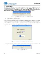
Verify that the USB cable is connected properly and that the power supply is on and connected properly
to the CDB5490U. Reset the board (press the 

RESET

 button on the board) and try to set up the USB con-

nection again.

After the serial port has been selected, the MCU will read the chip ID from the CS5490. The chip revision
number will be displayed in the Device field in the Start-Up Window. If the red "Unknown CHIP ID" is dis-
played, the user should check the power supply and clock to the CS5490, 

MODE

 jumper J15, and the

isolation jumpers J18 and J20, click the 

RESET

 button, and go back to the USB connection process.

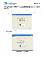
2.5

System

 Menu

The 

System

 pull-down provides three options: 

Setup CS5490

Calibration

, and 

Conversion

. Each window

provides a means to evaluate the different functions and performance of the CS5490 (see Figure 15).

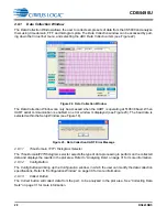
Figure 14.  Unknown Chip ID Error Message

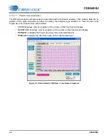
Figure 15.  

System

 Pull-down Options

Содержание CDB5490U

Страница 1: ...ltage Reference Access General Description The CDB5490U is an extensive tool designed to evaluate the functionality and performance of Cirrus Logic s CS5490 power measurement device Multiple analog input connection options configuration input fil ters direct and isolated digital interfaces multiple power supply options an onboard programmable microcontroller visual LEDs with an LCD panel make the ...

Страница 2: ...s current and complete All products are sold subject to the terms and conditions of sale supplied at the time of order acknowledgment including those pertaining to warranty indemnification and limitation of liability No responsibility is assumed by Cirrus for the use of this information including use of this information as the basis for manufacture or sale of any items or for infringement of paten...

Страница 3: ...ion 11 1 6 Typical Sensor Connections 12 1 7 Standalone Meter Application 15 2 SOFTWARE 16 2 1 Installation Procedure 16 2 2 Using the Software 16 2 3 Start up Window 17 2 4 Connect Menu 18 2 5 System Menu 19 2 6 Calibration Window 23 2 7 Conversion Window 25 2 8 Cirrus Test Window 27 Appendix A Bill Of Materials 37 Appendix B Schematics 39 Appendix C Layer Plots 42 ...

Страница 4: ...ndow 20 Figure 17 Calibration Window 23 Figure 18 Setup Window with 510638 Baud Rate 25 Figure 19 Conversion Collection Baud Rate Error 25 Figure 20 Conversion Window 26 Figure 21 Cirrus Test Pull down Options 27 Figure 22 Data Collection Window 28 Figure 23 Data Collection UART Error Message 28 Figure 24 Data Collection Output Window 29 Figure 25 Data Collection Configuration Window 30 Figure 26 ...

Страница 5: ...provides easy access to the internal registers of the CS5490 The software provides a means to display the on chip ADC performance in the time domain or frequency domain 1 2 Evaluation Board Overview The board is partitioned into two main sections analog and digital The analog section consists of the CS5490 passive anti aliasing filters and a high voltage section with an attenuation resistor networ...

Страница 6: ...11 to position VIN the input voltage signal is supplied from the screw terminals or XLR connections The CDB5490U evaluation board provides screw type terminals J4 to connect a high voltage line input By installing jumpers on J6 to position LINE and J11 to position GND the input voltage signal is supplied from the high voltage input Extreme care should be used when connecting high voltage signals t...

Страница 7: ...Vrms The CDB5490U evaluation board provides input shorting options for calibration and noise performance measurements With a jumper on J6 and J11 in the GND position the inputs are connected to analog ground GND GND LINE CS5490 CDB5490U NEUTRAL LINE J4 J11 J6 R5 1K C9 0 027UF C4 0 027UF R7 1K R6 1K R8 422K R12 422K R14 422K R15 422K J45 VIN VIN Figure 3 Voltage Channel High voltage Input 1k 4 422k...

Страница 8: ...e screw terminals or XLR connectors The CDB5490U evaluation board provides input shorting options for calibration and noise performance measurements With a jumper on J8 and J7 in the GND position the inputs are connected to analog ground GND Table 2 Current Channel Input Signal Selection INPUT Description J8 J7 IIN Selects External Low voltage Fully Differential Signal IIN Selects External Low vol...

Страница 9: ...n Communication to the CS5490 is provided through a standard UART It is necessary to establish commu nication with the MCU before serial port communication with the CS5490 see Figure 5 The CDB5490U board provides two UART communication options normal speed and low speed Table 3 provides the serial communication options for the UART Table 3 Serial Communication Options Figure 5 MCU Connection Windo...
Страница 10: ...e jumpers J18 and J20 in the RX to DIGITAL position and TX to DIGITAL position To en able the high speed digital isolators it is also necessary to install jumper J50 in the VDDA position To enable the low speed optical UART communication place jumpers J18 and J20 in the RX to OPTICAL position and TX to OPTICAL position The high speed digital isolators operate from DC to 150Mbps The low speed optic...

Страница 11: ... isolated sensors it is strongly recom mended that the CS5490 GND reference is connected to the neutral the non isolated current sensor is connected on neutral and the CS5490 is supplied by 3 3V isolated from AC line The DC DC converter U8 provides 1kVDC isolation while no isolation is provided for the 3 3V binding post connections If 3 3V is used from the binding post then the external 3 3VDC pow...

Страница 12: ...are well connected before the power source is turned on Ex treme care should be taken when connecting high voltage signals to the CDB5490U evaluation board In this configuration it is unnecessary to use a burden resistor A single anti alias filter is all that is required for the current channel Below the filter corner frequency the CS5490 inputs will see the same voltage that is across the shunt T...

Страница 13: ...nput voltage Vburden that the meter places on the system The optimum secondary voltage Vburden at the maximum current input should be 10 less than the maximum channel voltage of 250mVp with I channel PGA 10x The secondary voltage Vburden is determined by converting the primary current to the sec ondary current Then the secondary current Iburden can be converted into a voltage by Ohm s Law The seco...

Страница 14: ...gurations For more information see AN365 Using the CS5480 84 90 Energy Measurement IC with Rogowski Coil Current Sensors IIN IIN GND GND GND LINE CS5490 CDB5490U PHASE NEUTRAL J1 J4 J7 J8 J11 J6 R5 1K C5 0 033UF C6 0 033UF C9 0 027UF C4 0 027UF R11 NO POP R1 100 R2 100 R7 1K R6 1K R9 NO POP R13 NO POP R8 422K R12 422K R14 422K R15 422K R49 1K R50 1K C34 0 033UF C35 0 033UF J44 J46 R51 0 J45 J53 J5...

Страница 15: ... is connected to the CDB5490U board the standalone power meter function is disabled and the LCD on the CDB5490U will read Cirrus Logic CS5490 Eval GUI To re enable the standalone power meter feature close the GUI software The standalone power meter feature will initially show the voltage channels RMS register val ues V1rms N NNNNN and V2rms N NNNNN By clicking the onboard switch S2 the standalone ...

Страница 16: ...on to store the compressed folder 6 Click the Save button The Download complete window is displayed 7 Click the Open Folder button The location where the compressed folder is stored is displayed 8 Right click on the compressed folder and click Extract All 9 Select a location to extract the files 10 Navigate to the location where the extracted files are stored and double click on the setup exe file...

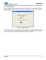
Страница 17: ...on number and copyright date The Start Up Window is dis played see Figure 10 At the top of the window a menu bar with menu items is displayed The menu bar has four menu items System Cirrus Test Connect and Quit Initially System and Cirrus Test are disabled After establishing a link to a data source the System and Cirrus Test items will become available Figure 10 GUI Start up Window ...

Страница 18: ...oll the C8051F342 microcontroller verifying the serial communication link is ready At this point the USB menu item is checked indicating that the PC has successfully communicated with the CDB5490U evaluation board The micro code version and device information are read from the board and displayed on the screen see Figure 12 Due to improvements to the software or new features being added the versio...

Страница 19: ...isplayed in the Device field in the Start Up Window If the red Unknown CHIP ID is dis played the user should check the power supply and clock to the CS5490 MODE jumper J15 and the isolation jumpers J18 and J20 click the RESET button and go back to the USB connection process 2 5 System Menu The System pull down provides three options Setup CS5490 Calibration and Conversion Each window provides a me...

Страница 20: ...on and are decoded Refer to the CS5490 data sheet for information on register functionality and definitions The Set up Window is segmented by function Each subsection may contain more than one CS5490 register in order to configure a particular function Updating the hexadecimal value of a register will change the def initions display according to the new hexadecimal value of the register s Likewise...

Страница 21: ...be modified by typing a hexadecimal value in the HEX field or by changing any of the values below the HEX field to the desired settings Although the CDB5490U software allows the user to modify any of the bits in the configuration registers changing certain reserved bits such as the NO_OSC bit of Config0 may cause the software and board to behave erratically This applies only to the CDB5490U evalua...

Страница 22: ...date rate of Epsilon is increased by reducing the zero crossings The register can be modified by typing the number of zero crossings 2 5 1 12 Epsilon The Epsilon section is used to display and adjust the Epsilon register the ratio of the AC line frequency to the output word rate The Epsilon register can be updated either through entering the AC line frequen cy in the Line Freq field or by entering...

Страница 23: ...al registers inside the CS5490 The register checksum updates automatically after single or continuous conversion has been performed The RegChk and SerialCtrl registers are displayed in hexadecimal form Please note that if the opto couplers are se lected as the isolation J18 J20 the maximum baud rate is 2400 The baud rate field applies only to UART serial communication and can be changed by the pul...

Страница 24: ... the CS5490 It is recommended to software reset the CS5490 before running calibrations because the initial values in the calibration registers will affect the results of the calibration A software reset will reset these registers back to the default values of zero offset and unity gain AC DC offset calibration should be per formed before gain calibration to ensure accurate results 2 6 3 1 Offset C...

Страница 25: ...sults of single and continuous conversions and the CS5490 status perform data averaging and use the power saving modes of the CS5490 The Conver sion Window can be accessed from the System menu pull down Conversion menu item The Conversion Window provides the active apparent and reactive energy calculations register results for each channel In addition the RMS power factor and peak signal amplitude...

Страница 26: ...s will be updated every N cycle where N is the number in the Samples to Average field The user should stop continuous conversion before leaving this window The Continuous Conversion button should not be used with BAUD rates less than 1200Hz in UART mode Using lower BAUD rates including the default 600 baud will result in overflowing the communication buf fer and cause other window errors communica...

Страница 27: ...his ensures the accuracy of the quadrature power Q and the reactive power QAVG cal culations Refer to the CS5490 data sheet for more details 2 7 6 Temperature Result The Temperature fields will display the current CS5490 die temperature in the top right corner of the Con version Window 2 7 7 Samples to Average The Samples to Average field allows the user to average a number of measurement results ...

Страница 28: ...ed within the Setup Window see Figure 18 2 8 1 1 Time Domain FFT Histogram Selector The Time Domain FFT Histogram selector selects the type of data processing to perform on the collected data and displays the results in the plot area Refer to Analyzing Data on page 31 for more information 2 8 1 2 Config Button The Config button will bring up the Configuration window in which the user can modify th...

Страница 29: ...n to return to the normal data plot or press the Zoom button again to zoom in farther 2 8 1 6 Channel Select Button After data collection the two buttons labeled as No Data will be replaced with Current and Voltage but tons allowing the user to choose the appropriate channel for display In the time domain mode an addi tional Overlay button will be present which allows the user to display all the c...

Страница 30: ...Blackman Harris Hanning 5 term Hodie and 7 term Hodie The 5 term Hodie and 7 term Hodie are windowing algorithms developed at Crystal Semiconductor now called Cirrus Logic 2 8 1 8 4 Histogram Bin Width This field determines the bin width when plotting histograms of the collected data Each vertical bar in the histogram plot will contain the number of output codes entered in this field Increasing th...

Страница 31: ... to begin collecting data 4 Once the data has been collected it can be analyzed printed or saved to disk 2 8 1 10 Analyzing Data The evaluation software provides three types of analysis tests Time Domain Frequency Domain and Histo gram The Time Domain analysis processes acquire conversions to produce a plot of magnitude versus con version sample number The Frequency Domain analysis processes acqui...

Страница 32: ...e of the cursor on the histogram MEAN Indicates the mean of the data sample set The mean is calculated using the following formula STD_DEV Indicates the standard deviation of the collected data set The standard deviation is calculated using the following formula VARIANCE Indicates the variance of the current data set The variance is calculated using the following formula MAXIMUM Indicates the maxi...

Страница 33: ...xis value of the cursor on the FFT display MAGNITUDE Displays the y axis value of the cursor on the FFT display S PN Indicates the signal to peak noise ratio decibels SINAD Indicates the signal plus noise plus distortion to noise plus distortion ratio decibels S D Indicates the signal to distortion ratio 4 harmonics are used in the calculations decibels SNR Indicates the signal to noise ratio firs...

Страница 34: ...nalysis type selector to Time Domain see Figure 28 The Time Domain plot includes COUNT Displays current x position of the cursor on the time domain display MAGNITUDE Displays current y position of the cursor on the time domain display MAXIMUM Indicates the maximum value of the collected data set MINIMUM Indicates the minimum value of the collected data set Figure 28 Data Collection Window Time Dom...

Страница 35: ...for data collection to a file 1 Provide the Time to Collect in seconds 2 If a delay before data collection is needed enter the time in seconds for the Delay 3 Select the voltage and current channel V and I 4 Browse to a directory and enter the file name of the desired file to save 5 Start the data collection by pressing the START button 6 The data collection status will be provided in Samples Coll...

Страница 36: ...ages In order to properly write a register it is necessary to set the Page Ad dress and Value to Write field and then press the WRITE button To read a register it is necessary to set the Page and Address and then press the READ button The register result will be displayed in the Value Read field To send a command to the CS5490 enter the command in the Command field and press the SEND button Refer ...

Страница 37: ... CON TERM BLOCK 2POS 5mm NPb BLU TH 2 J4 J27 ON SHORE TECHNOLOGY ED 100 2DS A 19 115 00016 Z1 A HDR 3x2 ML 1 CTR 062 S GLD NPb 1 J6 SAMTEC TSW 103 07 G D A 20 115 00257 Z1 A HDR 2x2 ML 1 093BD ST GLD NPb TH 3 J7 J8 J11 SAMTEC TSW 102 08 G D A 21 115 00009 Z1 A HDR 3x1 ML 1 062 ST GLD NPb TH 8 J15 J18 J20 J26 J38 J43 J50 J58 SAMTEC TSW 103 07 G S A 22 115 00012 Z1 A HDR 4x2 ML 1 CTR S GLD NPb 2 J17...

Страница 38: ...E 5001 A 52 065 00334 Z4 B2 IC CRUS ENER MEAS NPb SOIC16L 1 U1 CIRRUS LOGIC CS5490 ISZ B2 ECO898 ECO935 A 53 060 00319 Z1 A IC LNR VREG µPWR 150mA NPb SOT23 5 1 U2 NATIONAL SEMICONDUCTOR LP2985IM5 3 3 NOPB ECO813 A 54 060 00570 Z1 A IC ISOL 4CH 2 5kV 2 2 NPb SOIC16N 1 U3 SILICON LABORATORIES Si8442BB D IS1 A 55 175 00031 Z1 A OPT COUP TRANS 50 600 NPb DIP4 2 U4 U5 TOSHIBA TLP781 F A 56 062 00229 Z...

Страница 39: ... 11 B1 ECO832 ECO853 C CHGD Z3 TO CTES033V3 G CHGD DANGER LABEL A GARZA 4 8 11 Alan ZHA 4 8 11 ECO898 C1 A GARZA 9 15 11 Alan ZHA 9 15 11 CHGD U1 TO CS5490 INZ Rev B0 ECO935 C2 CHDG U1 TO CS5490 INZ B2 A GARZA 3 12 12 Alan Zha 3 12 12 1 2 3 4 J1 1 2 3 4 J7 1 2 3 4 J8 C5 0 027UF X7R C6 0 027UF X7R R11 2 2 NO POP R1 100 R2 100 R9 1K NO POP R13 1K NO POP 1 2 3 4 J3 1 2 J4 1 2 3 4 5 6 J6 HDR3X2 1 2 3 ...

Страница 40: ...3 4 7uF ELEC J39 J43 XIN J49 DO1 TEST2 J50 ASSY DWG 603 00483 Z1 PCB DWG 240 00483 Z1 SCHEMATIC DWG 600 00483 Z1 LBL SUBASSY PROD ID AND REV WIRE HOOK UP 6AWG STR BLU NPb L 1 5X 25TX 25T_TYPE_E_ MH1 MH2 MH3 MH4 MH5 1 FD1 1 FD2 1 FD3 SOCKET 1P 8134 HC 5P2 R55 130 C3 15pF COG 1 2 3 Z3 CTES033V3 G J57 VDDD J58 J48 SCREW PHILIPS 4 40THR PH 5 16 L Z PMSSS 440 0031 PH MH6 MH7 SHUNT_2P 15 29 1025 C10 0 1...

Страница 41: ...5 13 DB6 14 DB7 15 BLA 16 BLK LCD1 LCD 16P LMB162AFC 2 LCD R37 0 R38 0 R42 0 C22 0 1uF X7R C23 0 1uF X7R C24 47uF ELEC C25 0 1uF X7R 1 5V 2 D 3 D 4 GND 5 GND 6 GND J24 292304 1 USB C26 22pF 4 3 1 2 D5 SP0503BAHTG 1 2 3 4 5 6 7 8 9 10 J25 HDR5X2 JTAG C2 1 5 3 S1 RESET R44 1K C27 0 1uF X7R C28 1UF X7R R45 1K R46 1K J26 1 2 J27 1 5 3 S2 SWITCH R47 5 1K C29 0 1uF X7R 1 2 D6 RED EVENT R48 680 1 2 Z2 6 ...

Страница 42: ...CDB5490U 42 DS923DB5 APPENDIX C LAYER PLOTS Figure 36 Top Silkscreen ...

Страница 43: ...CDB5490U DS923DB5 43 Figure 37 Top Routing ...

Страница 44: ...CDB5490U 44 DS923DB5 Figure 38 Bottom Routing ...

Страница 45: ...CDB5490U DS923DB5 45 Figure 39 Solder Paste Mask ...

Страница 46: ...DB1 APR 2011 Initial Release DB2 DEC 2011 Updated screen shots and circuit diagrams to align with B0 silicon DB3 JAN 2012 Corrected typographical errors DB4 MAR 2012 Updated content DB5 APR 2012 Updated screen shots and circuit diagrams to align with B2 silicon ...

Отзывы: