— 3 —
BT
BS
VCC6
TU
H/L
BU
VREF
GND
16
15
14
13
12
11
10
9
1
2
3
4
5
6
7
8
Vcc
BS
BT
IN
OUT
TU
H/L
U/V
VREF
U1
U2
VL1
VL2
VH1
VH2
GND
R500
R501
R502
IC500 MSC1169MS-K
Function
CIRCUIT DESCRIPTION
TUNING VOLTAGE GENERATOR
Table 1
Figure 2
Figure 1
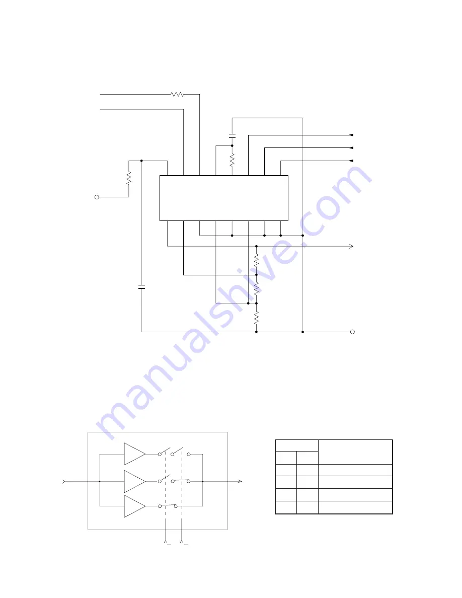
This circuit generates the DC tuning voltage BT for selecting a channel with a TU pulse being output from
IC700.
IC500 has 3 circuits for converting pulses to voltages; it selects one of VHF-L, VHF-H, or UHF, and
causes the tuning voltage to be output from the OUT terminal (pin 12). Figure 2 and Table 1 show the
conditions for selection.
IC500
TU
OUT(BT)
U/V H/L
VHF
-H
UHF
VHF
-L
11
9
10
12
U/V
L
L
H
H
H/L
L
H
L
H
Inputs
VHF-L receiving
VHF-H receiving
UHF receiving
UHF receiving
Содержание TV-600B
Страница 11: ... 15 WIRING DIAGRAM TOP VIEWS 1 17 1 17 A D PCB Linear PCB ...
Страница 16: ... 27 A D 11 12 TP6 ...


