


Under no circumstance may a P pin receive any voltage that is higher than the interface’s
Vcc (operating voltage). This is 3.3VDC for the ESP32. If this limit is exceeded, irreparable
damage will occur to both the interface and the base board’s drivers.
The D pins are driven by the high-current driver chips on the board. These are automotive
grade and contain protection circuitry to handle overtemperature, overcurrent, and other fault
situations. The D pins will output the matching voltage associated with its VA or VB bank power
input when ON, therefore only Active-High configurations can be implemented (do not use
Active Low settings in BruControl Device Elements).
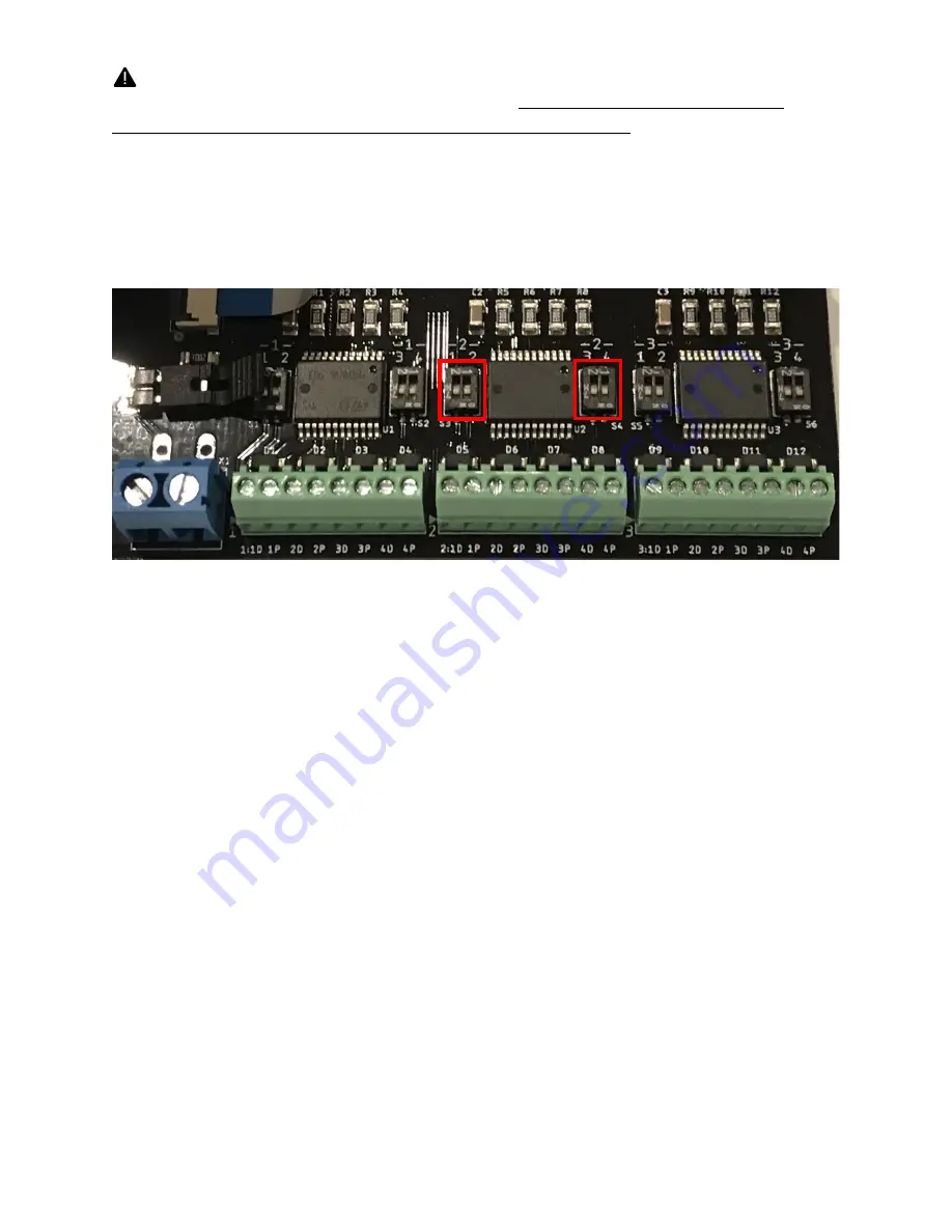
Figure 3: Terminal 2 with Driver Connect Switches for 1, 2, 3, and 4 pins
On either side of the driver chips are pairs of miniature slide switches. These switches connect
the respective P pin to the driver chip input, thereby switching the driver output (D pin) in
accordance with the P pin. These are defaulted in the ON position, but the user may opt to
switch them OFF in cases where the driver output will not be used or where complete removal
of the driver from the circuit is desired. The P pins are connected to the driver input, which is
also connected to ground via a 100k ohm resistor, so this should not normally be needed, but
the option exists should the P I/O pin not work as expected. Turning these switches OFF only
disable the driver output terminal (D pin) – they have no effect on the P pin. The switch location
is aligned with the I/O terminal block it affects and are labeled. The switch is in the ON position
when the switch is pointed toward the I/O terminals, also labeled ON on the switch body. These
switches are delicate and should be gently switched with an appropriate flat blade screwdriver.
All switches are shipped ON (closed) as their default state.
Figure 4 below depicts how the interface, slide switch, drivers, P and D pins are interconnected.